


 American Made Advocacy: Smart Policies Can Ensure AI Data Centers Are Secure
 Beyond the Board: Early Engagement Means Faster Prototyping for Defense Programs
 Defense Speak Interpreted: The Autonomous Plane Battle—Skyborg Vs. Loyal Wingman


Novel Laser Technology for Microchip-Size Chemical Sensors
December 11, 2018 | TU WienEstimated reading time: 3 minutes
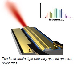
Most lasers have only one color. All the photons it emits have exactly the same wavelength. However, there are also lasers whose light is more complicated. If it consists of many different frequencies, with equal intervals in between, just like the teeth of a comb, it is referred to as a "frequency comb". Frequency combs are perfect for detecting a variety of chemical substances.
At TU Wien (Vienna), this special type of laser light is now used to enable chemical analysis on tiny spaces—it is a millimeter-format chemistry lab. With this new patent-pending technology, frequency combs can be created on a single chip in a very simple and robust manner. This work has now been presented in the journal "Nature Photonics".
A Comb with a Nobel Prize
Frequency combs have been around for years. In 2005, the Nobel Prize for Physics was awarded for this. "The exciting thing about them is that it is relatively easy to build a spectrometer with two frequency combs," explains Benedikt Schwarz, who heads the research project. "It is possible to make use of beats between different frequencies, similar to those that occur in acoustics, if you listen to two different tones with similar frequency. We use this new method, because it does not require any moving parts and allows us to develop a miniature chemistry lab on a millimetre scale."
At the Vienna University of Technology, frequency combs are produced with quantum cascade lasers. These special lasers are semiconductor structures that consist of many different layers. When electrical current is sent through the structure, the laser emits light in the infrared range. The properties of the light can be controlled by tuning the geometry of the layer structure.
"With the help of an electrical signal of a specific frequency, we can control our quantum cascade lasers and make them emit a series of light frequencies, which are all coupled together," says Johannes Hillbrand, first author of the publication. The phenomenon is reminiscent of swings on a rocking frame—instead of pushing individual swings, one can make the scaffolding wobble at the right frequency, causing all the swings to oscillate in certain coupled patterns. "The big advantage of our technology is the robustness of the frequency comb," says Benedikt Schwarz. Without this technique, the lasers are extremely sensitive to disturbances, which are unavoidable outside the lab - such as temperature fluctuations, or reflections that send some of the light back into the laser. "Our technology can be realized with very little effort and is therefore perfect for practical applications even in difficult environments. Basically, the components we need can be found in every mobile phone", says Schwarz.
The Molecular Fingerprint
The fact that the quantum cascade laser generates a frequency comb in the infrared range is crucial, because many of the most important molecules can best be detected by light in this frequency range. "Various air pollutants, but also biomolecules, which play an important role in medical diagnostics, absorb very specific infrared light frequencies. This is often referred to as the optical fingerprint of the molecule, "explains Johannes Hillbrand. "So, when we measure, which infrared frequencies are absorbed by a gas sample, we can tell exactly which substances it contains."
Measurements in the Microchip
"Because of its robustness, our system has a decisive advantage over all other frequency comb technologies: it can be easily miniaturized," says Benedikt Schwarz. "We do not need lens systems, no moving parts and no optical isolators, the necessary structures are tiny. The entire measuring system can be accommodated on a chip in millimeter format."
This results in spectacular application ideas: one could place the chip on a drone and measure air pollutants. Chips glued to the wall could search for traces of explosive substances in buildings. The chips could be used in medical equipment to detect diseases by analyzing chemicals in the respiratory air.
The new technology has already been patented. "Other research teams are already highly interested in our system. We hope that it will soon be used not only in academic research, but also in everyday applications, "says Benedikt Schwarz.
Share on:


Testimonial
"In a year when every marketing dollar mattered, I chose to keep I-Connect007 in our 2025 plan. Their commitment to high-quality, insightful content aligns with Koh Young’s values and helps readers navigate a changing industry. "
Brent Fischthal - Koh YoungSuggested Items
Nvidia’s Blackwell Chips Made in Arizona Still Head to Taiwan for Final Assembly
10/27/2025 | I-Connect007 Editorial TeamNvidia has begun production of its next-generation Blackwell GPUs in the United States, but the company still depends heavily on Taiwan to complete the process, The Register reported.
American Standard Circuits Launches 50th 77-Second Webinar
10/27/2025 | American Standard CircuitsAnaya Vardya, President and CEO of American Standard Circuits/ASC Sunstone Circuits is pleased to announce that they have recently unveiled their 50th 77-second webinar.
KYZEN Brings Reliability to Life at productronica 2025 with ANALYST² Process Control Demos
10/22/2025 | KYZEN'KYZEN, the global leader in innovative environmentally responsible cleaning chemistries, will exhibit at productronica 2025, November 18–21 in Munich, Germany, where the company will put a spotlight on its award-winning KYZEN ANALYST² process control system in Hall A4, Stand 450.
SCHMID Group Secures Major Orders for AI Server PCB Production Equipment
10/22/2025 | SCHMID GroupSCHMID Group, a global equipment maker and solution provider for Printed Circuit Boards (PCB) and IC-Substrate manufacturing – announced the successful acquisition of two significant orders in the fast-growing field of PCB for artificial intelligence (AI) server applications. So called AI-Server-Boards.
SEMICON Japan 2025 to Spotlight Sustainability in AI and Semiconductor Innovation
10/22/2025 | SEMISEMICON Japan 2025, the largest gathering of leaders from the microelectronics manufacturing supply chain in Japan, will bring together more than 1,200 exhibitors showcasing semiconductor solutions from December 17-19 at Tokyo Big Sight.