


 Dan’s Biz Bookshelf: ‘Atomic Habits’
 Happy’s Tech Talk #48: Digital Twins—Integrating Design and Manufacturing
 The Chemical Connection: The Consequences of Additive Metallizing on Etching Steps


UNSW scientists have shown that their pioneering single atom technology can be adapted to building 3D silicon quantum chips—with precise interlayer alignment and highly accurate measurement of spin states. The 3D architecture is considered a major step in the development of a blueprint to build a large-scale quantum computer.
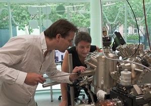
UNSW researchers at the Centre of Excellence for Quantum Computation and Communication Technology (CQC2T) have shown for the first time that they can build atomic precision qubits in a 3D device – another major step towards a universal quantum computer.
The researchers, led by 2018 Australian of the Year and Director of CQC2T Professor Michelle Simmons, have demonstrated that they can extend their atomic qubit fabrication technique to multiple layers of a silicon crystal—achieving a critical component of the 3D chip architecture that they introduced to the world in 2015. This new research is published today in Nature Nanotechnology.
The group is the first to demonstrate the feasibility of an architecture that uses atomic-scale qubits aligned to control lines—which are essentially very narrow wires—inside a 3D design.
What’s more, team members were able to align the different layers in their 3D device with nanometer precision—and showed they could read out qubit states with what’s called 'single shot', i.e. within one single measurement, with very high fidelity.
“This 3D device architecture is a significant advancement for atomic qubits in silicon,” says Professor Simmons.
“To be able to constantly correct for errors in quantum calculations—an important milestone in our field—you have to be able to control many qubits in parallel.
“The only way to do this is to use a 3D architecture, so in 2015 we developed and patented a vertical crisscross architecture. However, there were still a series of challenges related to the fabrication of this multi-layered device. With this result we have now shown that engineering our approach in 3D is possible in the way we envisioned it a few years ago.”
In this paper, the team has demonstrated how to build a second control plane or layer on top of the first layer of qubits.
“It’s a highly complicated process, but in very simple terms, we built the first plane, and then optimised a technique to grow the second layer without impacting the structures in first layer,” explains CQC2T researcher and co-author, Dr Joris Keizer.
“In the past, critics would say that that’s not possible because the surface of the second layer gets very rough, and you wouldn’t be able to use our precision technique anymore—however, in this paper, we have shown that we can do it, contrary to expectations.”
The team members also demonstrated that they can then align these multiple layers with nanometer precision.
“If you write something on the first silicon layer and then put a silicon layer on top, you still need to identify your location to align components on both layers. We have shown a technique that can achieve alignment within under five nanometers, which is quite extraordinary,” Dr Keizer says.
Lastly, the researchers were able to measure the qubit output of the 3D device single shot – i.e. with a single, accurate measurement, rather than having to rely on averaging out millions of experiments.
“This will further help us scale up faster,” Dr Keizer explains.
Towards Commercialization
Professor Simmons says that this research is a milestone in the field.
“We are working systematically towards a large-scale architecture that will lead us to the eventual commercialization of the technology.
“This is an important development in the field of quantum computing, but it’s also quite exciting for SQC,” says Professor Simmons, who is also the founder and a director of SQC.
Since May 2017, Australia’s first quantum computing company, Silicon Quantum Computing Pty Limited (SQC), has been working to create and commercialise a quantum computer based on a suite of intellectual property developed at CQC2T and its own proprietary intellectual property.
“While we are still at least a decade away from a large-scale quantum computer, the work of CQC2T remains at the forefront of innovation in this space. Concrete results such as these reaffirm our strong position internationally,” she concludes.


