


 Global PCB Connections: Rigid-flex and Flexible PCBs—The Backbone of Modern Electronics
 Flexible Thinking: The Key to a Successful Flex Circuit Design Transfer
 Happy’s Tech Talk #29: Bend-to-Install Semi-flex FR-4


AT&S: Innovators for Electromobility and Automated Driving
January 18, 2019 | AT&SEstimated reading time: 3 minutes
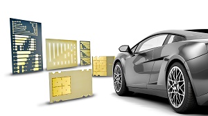
Electromobility and automated driving are the two defining trends in the automotive industry with high growth potential, but also technological challenges. For example, hybrid and/or electric powertrains require, among other things, efficient power electronics for the major subsystems such as inverters, on-board chargers or DC/DC converters. Finally, the implementation of electromobility also requires efficient, space-saving and reliable connection and packaging solutions. On the other hand, new high-performance sensor systems with sensor fusion and high-speed communication are required along the way to autonomous driving, all whilst maintaining functional safety and security. AT&S addresses all of these key automotive trends with innovative connection and packaging solutions.
Efficient Power
Electromobility continues to make headway, driven by legal requirements in all key regions – led by China. To date in the EU, the target of 95 g CO2/km has been the fleet average for 2021. According to a recent EU compromise, new cars in the EU are to emit another 37.5% less carbon dioxide by 2030 than in the comparable year 2021. This cannot be achieved without high-voltage electrification and mild hybrid vehicles with a 48V on-board power supply – and this is where efficient power electronics play a central role. AT&S expects above-average growth in electromobility applications over the next few years and is focussing here amongst other things on embedded power technologies – in other words, the embedding of power semiconductors such as MOSFETs in PCBs. Key benefits of ECP (embedded component packaging) over conventional PCB assembly include significant miniaturisation thanks to higher integration, improved reliability and superior thermal performance. In addition, ECP facilitates integrated EMI shielding and supports the adaptation of different coefficients of thermal expansion (CTE) for rapid and easy system integration.
As silicon-based solutions slowly reach their limits, the use of wide-band gap materials such as GaN promises more efficient power conversion, with higher efficiency and higher power density. Working closely with partners, AT&S has successfully reduced both the dimensions and the cost of these new components, thereby contributing to the faster adaption of the new technologies.
Automated Driving Requires High-Speed Communication and Sensor Fusion
The second megatrend in the automotive industry is automated driving. Automated or autonomous driving constitutes a great potential for the microelectronics industry. By way of illustration, the PCB market for these applications is currently growing at around 5.5% per annum. By 2020, the proportion of costs of electronic components in cars is expected to rise to 35%, and even to 50% by 2030 (source: Statista 2018).
With the increasing degree of automation and thus more sophisticated advanced driver assistance systems (ADAS), the need for sensors and different sensor technologies is also increasing in cars. Whilst a combination of camera and radar systems is sufficient up to level 2, from level 3 lidar also plays a crucial role.
Due to the ever higher frequencies such as for the radar, the traces on the circuit boards must also be regarded as RF components and designed accordingly. AT&S is a world leader in this field and has developed PCBs that deliver the necessary and also cost-efficient performance in the frequency range up to 80GHz. For example, these technologies form the basis for high-performance radar components (long-range radar with 77/79GHz) in advanced driver assistance systems – an indispensable prerequisite for autonomous driving.
The key criteria is a fast, interference-free signal transmission with minimal losses. The losses can be devided into dielectric, resistive, reflection-based and losses generated by emissions. For example, the RF signal in the PCB is influenced by various parameters such as conductor length, base material (loss factor and dielectric constant), reflections due to drilling, impedance matching, crosstalk and interference from external sources (EMC shielding).
AT&S addresses all these aspects. By way of example, AT&S is working intensively on new materials to further reduce the dielectric constant and the loss factor. Other innovative solutions include for example very thin copper foils with low roughness (with sufficient adhesion) for maximum speed or asymmetric hybrid or sandwich structures (e.g. FR4 for the digital layer and ceramic materials such as PTFE for the high-speed layer) for cost-effective PCB technologies up to frequencies of 80GHz.
Share on:


Testimonial
"Our marketing partnership with I-Connect007 is already delivering. Just a day after our press release went live, we received a direct inquiry about our updated products!"
Rachael Temple - AlltematedSuggested Items
Closing the Loop on PCB Etching Waste
09/09/2025 | Shawn Stone, IECAs the PCB industry continues its push toward greener, more cost-efficient operations, Sigma Engineering’s Mecer System offers a comprehensive solution to two of the industry’s most persistent pain points: etchant consumption and rinse water waste. Designed as a modular, fully automated platform, the Mecer System regenerates spent copper etchants—both alkaline and acidic—and simultaneously recycles rinse water, transforming a traditionally linear chemical process into a closed-loop system.
Driving Innovation: Depth Routing Processes—Achieving Unparalleled Precision in Complex PCBs
09/08/2025 | Kurt Palmer -- Column: Driving InnovationIn PCB manufacturing, the demand for increasingly complex and miniaturized designs continually pushes the boundaries of traditional fabrication methods, including depth routing. Success in these applications demands not only on robust machinery but also sophisticated control functions. PCB manufacturers rely on advanced machine features and process methodologies to meet their precise depth routing goals. Here, I’ll explore some crucial functions that empower manufacturers to master complex depth routing challenges.
Trouble in Your Tank: Minimizing Small-via Defects for High-reliability PCBs
08/27/2025 | Michael Carano -- Column: Trouble in Your TankTo quote the comedian Stephen Wright, “If at first you don’t succeed, then skydiving is not for you.” That can be the battle cry when you find that only small-diameter vias are exhibiting voids. Why are small holes more prone to voids than larger vias when processed through electroless copper? There are several reasons.
The Government Circuit: Navigating New Trade Headwinds and New Partnerships
08/25/2025 | Chris Mitchell -- Column: The Government CircuitAs global trade winds continue to howl, the electronics manufacturing industry finds itself at a critical juncture. After months of warnings, the U.S. Government has implemented a broad array of tariff increases, with fresh duties hitting copper-based products, semiconductors, and imports from many nations. On the positive side, tentative trade agreements with Europe, China, Japan, and other nations are providing at least some clarity and counterbalance.
How Good Design Enables Sustainable PCBs
08/21/2025 | Gerry Partida, Summit InterconnectSustainability has become a key focus for PCB companies seeking to reduce waste, conserve energy, and optimize resources. While many discussions on sustainability center around materials or energy-efficient processes, PCB design is an often overlooked factor that lies at the heart of manufacturing. Good design practices, especially those based on established IPC standards, play a central role in enabling sustainable PCB production. By ensuring designs are manufacturable and reliable, engineers can significantly reduce the environmental impact of their products.