


 Driving Innovation: Mechanical and Optical Processes During Rigid-flex Production
 It’s Only Common Sense: Your Biggest Competitor Is Complacency
 The Chemical Connection: Onshoring PCB Production—Daunting but Certainly Possible


A Tip for Future Nanoscale Sensing
February 27, 2019 | A*STAREstimated reading time: 2 minutes
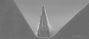
Commercially-available diamond tips used in atomic force microscopy (AFM) could help make quantum nanoscale sensing cost-effective and practical, A*STAR researchers have found.
The idea of using ‘color centers’, optically-active atomic defects in diamond, as a probe for taking highly sensitive nanoscale measurements of quantities such as elecromagnetic field, temperature, or strain is well known. In practice, however, these experiments often required the expensive fabrication of custom-designed diamond nanostructures and it is a challenge to collect the very weak optical signal that the color centers produce.
Now, a recent study published by Victor Leong, and colleagues from A*STAR’s Institute of Materials Research and Engineering, and the Institute of High Performance Computing, suggests that use of commercial pyramid-shaped diamond AFM tips that contain silicon vacancy centers could help. The approach has several advantages.
Firstly, the team’s experiments with a confocal microscope and diamond tips arranged in different orientations show that the pyramid shape of the diamond tip acts as a highly efficient collector of the weak infrared (738 nanometer) photoluminescence generated by the color center. Due to geometric effects, a larger portion of the emitted photoluminescence was channeled to the base of pyramid, resulting in a signal up to eight times stronger than other directions. In the experiments, the base of the tip was attached to a silicon nitride cantilever, transparent to the infrared light, so that the photoluminescence was able to pass through and be collected by a spectrophotometer.
“In many nanosensing applications, the signal is inherently very weak and this poses a fundamental limit to the sensitivity,” explained Leong. “The ability to collect and detect a larger signal improves many performance metrics such as minimum detectable signal, resolution and measurement time, for example.”
Secondly, these diamond tips are commercially available and compatible with AFM and microscope equipment, offering a path to practical implementation. “These off-the-shelf diamond AFM tips are easily available and inexpensive. They cost around SGD 100 each,” commented Leong. “If they contain color centers with suitable optical properties, they could be a low-cost substitute for other diamond nanoprobes. The lower cost and easy availability could help promote the rapid development and uptake of quantum technological applications.”
The extremely small size of the diamond tips, which have a tip radius of approximately 10 nanometers and length of around 15 micrometers, means that they can be brought extremely close to the sample to be studied, maximizing measurement sensitivity and spatial resolution. “These diamond tips could potentially be used in sensing applications that are challenging to perform with other diamond structures, for example, mapping the electromagnetic properties of deep trenches or the space around closely-placed nanostructures,” commented Leong.
To date, the team has focused on investigating diamond tips featuring silicon vacancy color centers but Leong says that it is possible to also introduce nitrogen vacancy color centers which are popular in magnetometry studies. “The batch of diamond tips discussed in the paper1 were manufactured in a nominally nitrogen-free process and thus had many silicon vacancy centers but very few nitrogen vacancy centers,” explained Leong. “However, other separate batches of diamond tips we obtained, contained high concentrations of nitrogen vacancy centers.”
Now that the team has shown that enhanced optical readout is possible from the diamond tips, the next stage of the research will be to optimize performance and then perform some actual sensing experiments “We plan to deploy these tips in practical nanosensing applications. Current ideas include nanoscale magnetic sensing and surface studies,” said Leong.
Share on:


Testimonial
"Advertising in PCB007 Magazine has been a great way to showcase our bare board testers to the right audience. The I-Connect007 team makes the process smooth and professional. We’re proud to be featured in such a trusted publication."
Klaus Koziol - atgSuggested Items
Defense Speak Interpreted: The Autonomous Plane Battle—Skyborg Vs. Loyal Wingman
10/07/2025 | Dennis Fritz -- Column: Defense Speak InterpretedI’m awaiting the updates for the U.S. Air Force's Skyborg and Loyal Wingman airborne driverless vehicles. As the hype of self-driving cars has given way to more mundane autonomous activities, so too has the hype of uncrewed planes given way to reality. In cars, the SAE International association classifies degrees of autonomy from 0 to 5, as do some defense aerospace applications of unmanned flight, which have been reduced to practice, while others remain under development.
Schweizer Ends Staff Restructuring Measures and Short-Time Working at the Schramberg Site
10/01/2025 | Schweizer Electronic AGSchweizer Electronic AG has implemented comprehensive measures to adjust its cost and personnel structure at its Schramberg site due to strong market fluctuations in the automotive and industrial electronics sector. Thanks to the successful restructuring, short-time working can now be ended with immediate effect. A stable order situation is expected for the fourth quarter, with signs of growth momentum returning in 2026.
Global Sourcing Spotlight: Finding the Balance Between Cost and Quality
09/24/2025 | Bob Duke -- Column: Global Sourcing SpotlightIn global sourcing, pursuing lower costs often takes center stage. It’s the shiny lure that gets buyers to cast their lines into unfamiliar waters. But seasoned professionals know that in the long run, sourcing is less about price tags and more about value. The real magic—and margin—lies in finding the balance between cost and quality.
I-Connect007 Editor’s Choice: Five Must-Reads for the Week
08/15/2025 | Marcy LaRont, I-Connect007In our industry, my top reads include Prashant Patel’s overview and argument for reshoring, which I found to be a great general overview and breakdown. In further support of the onshoring/reshoring message, I’m highlighting Nolan Johnson’s interview on the survey and report by the Reshoring Initiative. Check out my interview with USPAE’s Jim Will on the state of the flat panel display (FPD) industry and the risks associated with it for U.S. defense and critical infrastructure products.
Global Electronics Industry Remains Under Pressure from Rising Costs
08/04/2025 | Global Electronics AssociationThe global electronics manufacturing supply chain remains under pressure from rising costs, with 61% of firms reporting higher material costs and 54% noting increased labor expenses. according to the Global Electronics Association’s Sentiment of the Global Electronics Manufacturing Supply Chain Report.