


 Driving Innovation: Mechanical and Optical Processes During Rigid-flex Production
 It’s Only Common Sense: Your Biggest Competitor Is Complacency
 The Chemical Connection: Onshoring PCB Production—Daunting but Certainly Possible


Scientists Develop Printable Water Sensor
March 5, 2019 | DESYEstimated reading time: 3 minutes
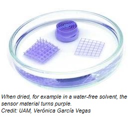
A new, versatile plastic-composite sensor can detect tiny amounts of water. The 3D printable material, developed by a Spanish-Israeli team of scientists, is cheap, flexible and non-toxic and changes its colour from purple to blue in wet conditions. The researchers lead by Pilar Amo-Ochoa from the Autonomous University of Madrid (UAM) used DESY’s X-ray light source PETRA III to understand the structural changes within the material that are triggered by water and lead to the observed colour change. The development opens the door to the generation of a family of new 3D printable functional materials, as the scientists write in the journal Advanced Functional Materials (early online view).
In many fields, from health to food quality control, environmental monitoring and technical applications, there is a growing demand for responsive sensors which show fast and simple changes in the presence of specific molecules. Water is among the most common chemicals to be monitored. “Understanding how much water is present in a certain environment or material is important,” explains DESY scientist Michael Wharmby, co-author of the paper and head of beamline P02.1 where the sensor-material was examined with X-rays. “For example, if there is too much water in oils they may not lubricate machines well, whilst with too much water in fuel, it may not burn properly.”
The functional part of the scientists’ new sensor-material is a so-called copper-based coordination polymer, a compound with a water molecule bound to a central copper atom. “On heating the compound to 60 degrees Celsius, it changes colour from blue to purple”, reports Pilar Amo-Ochoa. “This change can be reversed by leaving it in air, putting it in water, or putting it in a solvent with trace amounts of water in it.” Using high-energy X-rays from DESY's research light source PETRA III at the experimental station P02.1, the scientists were able to see that in the sample heated to 60 degrees Celsius, the water molecule bound to the copper atoms had been removed. This leads to a reversible structural reorganisation of the material, which is the cause of the colour change.
“Having understood this, we were able to model the physics of this change,” explains co-author José Ignacio Martínez from the Institute for Materials Science in Madrid (ICMM-CSIC). The scientists were then able to mix the copper compound into a 3D printing ink and printed sensors in several different shapes which they tested in air and with solvents containing different amounts of water. These tests showed that the printed objects are even more sensitive to the presence of water than the compound by itself, thanks to their porous nature. In solvents, the printed sensors could already detect 0.3 to 4 per cent of water in less than two minutes. In air, they could detect a relative humidity of 7 per cent.
If it is dried, either in a water free solvent or by heating, the material turns back to purple. A detailed investigation showed that the material is stable even over many heating cycles, and the copper compounds are evenly distributed throughout the printed sensors. Also, the material is stable in air over at least one year and also at biological relevant pH ranges from 5 to 7. “Furthermore, the highly versatile nature of modern 3D printing means that these devices could be used in a huge range of different places,” emphasises co-author Shlomo Magdassi from The Hebrew University of Jerusalem. He adds that the concept could be used to develop other functional materials as well.
“This work shows the first 3D printed composite objects created from a non-porous coordination polymer,” says co-author Félix Zamora from the Autonomous University of Madrid. “It opens the door to the use of this large family of compounds that are easy to synthesize and exhibit interesting magnetic, conductive and optical properties, in the field of functional 3D printing.”
The Autonomous University of Madrid, the Hebrew University of Jerusalem, the Nanyang Technological University in Singapore, the Institute for Materials Science in Madrid and DESY contributed to this research.
Share on:


Testimonial
"In a year when every marketing dollar mattered, I chose to keep I-Connect007 in our 2025 plan. Their commitment to high-quality, insightful content aligns with Koh Young’s values and helps readers navigate a changing industry. "
Brent Fischthal - Koh YoungSuggested Items
WestDev Announces Advanced Thermal Analysis Integration for Pulsonix PCB Design Suite
10/29/2025 | WestDev Ltd.Pulsonix, the industry-leading PCB design software from WestDev Ltd., announced a major enhancement to its design ecosystem: a direct interface between Pulsonix and ADAM Research's TRM (Thermal Risk Management) analysis software.
Designers Notebook: Power and Ground Distribution Basics
10/29/2025 | Vern Solberg -- Column: Designer's NotebookThe principal objectives to be established during the planning stage are to define the interrelationship between all component elements and confirm that there is sufficient surface area for placement, the space needed to ensure efficient circuit interconnect, and to accommodate adequate power and ground distribution.
Episode 6 of Ultra HDI Podcast Series Explores Copper-filled Microvias in Advanced PCB Design and Fabrication
10/15/2025 | I-Connect007I-Connect007 has released Episode 6 of its acclaimed On the Line with... American Standard Circuits: Ultra High Density Interconnect (UHDI) podcast series. In this episode, “Copper Filling of Vias,” host Nolan Johnson once again welcomes John Johnson, Director of Quality and Advanced Technology at American Standard Circuits, for a deep dive into the pros and cons of copper plating microvias—from both the fabricator’s and designer’s perspectives.
Nolan’s Notes: Tariffs, Technologies, and Optimization
10/01/2025 | Nolan Johnson -- Column: Nolan's NotesLast month, SMT007 Magazine spotlighted India, and boy, did we pick a good time to do so. Tariff and trade news involving India was breaking like a storm surge. The U.S. tariffs shifted India from one of the most favorable trade agreements to the least favorable. Electronics continue to be exempt for the time being, but lest you think that we’re free and clear because we manufacture electronics, steel and aluminum are specifically called out at the 50% tariff levels.
MacDermid Alpha & Graphic PLC Lead UK’s First Horizontal Electroless Copper Installation
09/30/2025 | MacDermid Alpha & Graphic PLCMacDermid Alpha Electronics Solutions, a leading supplier of integrated materials and chemistries to the electronics industry, is proud to support Graphic PLC, a Somacis company, with the installation of the first horizontal electroless copper metallization process in the UK.