


 Driving Innovation: Mechanical and Optical Processes During Rigid-flex Production
 It’s Only Common Sense: Your Biggest Competitor Is Complacency
 The Chemical Connection: Onshoring PCB Production—Daunting but Certainly Possible


Graphene Quantum Dots for Single Electron Transistors
March 7, 2019 | National Research University Higher School of EconomicsEstimated reading time: 1 minute
Scientists from the Higher School of Economics, Manchester University, the Ulsan National Institute of Science & Technology and the Korea Institute of Science and Technology have developed a novel technology, which combines the fabrication procedures of planar and vertical heterostructures in order to assemble graphene-based high-quality single-electron transistors. This technology could considerably expand the scope of research on two-dimensional materials by introducing a broader platform for the investigation of various devices and physical phenomena.
In the study, it was demonstrated that high-quality graphene quantum dots (GQDs), regardless of whether they were ordered or randomly distributed, could be successfully synthesised in a matrix of monolayer hexagonal boron nitride (hBN). Here, the growth of GQDs within the layer of hBN was shown to be catalytically supported by the platinum (Pt) nanoparticles distributed in-between the hBN and supporting oxidised silicon (SiO2) wafer, when the whole structure was treated by the heat in the methane gas (CH4). It was also shown, that due to the same lattice structure (hexagonal) and small lattice mismatch (~1.5%) of graphene and hBN, graphene islands grow in the hBN with passivated edge states, thereby giving rise to the formation of defectless quantum dots embedded in the hBN monolayer.
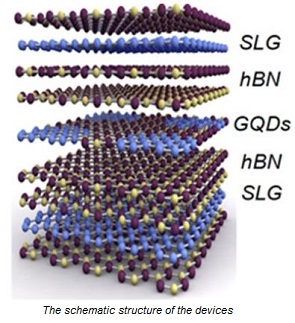
The Schematic Structure of the Devices
Such planar heterostructures incorporated by means of standard dry-transfer as mid-layers into the regular structure of vertical tunnelling transistors (Si/SiO2/hBN/Gr/hBN/GQDs/hBN/Gr/hBN; here Gr refers to monolayer graphene and GQDs refers to the layer of hBN with the embedded graphene quantum dots) were studied through tunnel spectroscopy at low temperatures (3He, 250mK). The study demonstrated where the manifestation of well-established phenomena of the Coulomb blockade for each graphene quantum dot as a separate single electron transmission channel occurs.
"Although the outstanding quality of our single electron transistors could be used for the development of future electronics," explains study co-author Davit Ghazaryan, associate professor at the HSE Faculty of Physics, and Research Fellow at the Institute of Solid State Physics (RAS). ‘This work is most valuable from a technological standpoint as it suggests a new platform for the investigation of physical properties of various materials through a combination of planar and van der Waals heterostructures.’
Share on:


Testimonial
"Our marketing partnership with I-Connect007 is already delivering. Just a day after our press release went live, we received a direct inquiry about our updated products!"
Rachael Temple - AlltematedSuggested Items
LPKF Delivers Key Strategic Technology to Fraunhofer's Glass Panel Technology Group
10/29/2025 | LPKFLPKF Laser & Electronics SE is one of the initiators of the Glass Panel Technology Group (GPTG), a consortium encompassing the entire process chain for advanced semiconductor packaging with glass substrates.
On the Line With… Ultra HDI Podcast—Episode 7: “Solder Mask: Beyond the Traces,” Now Available
10/29/2025 | I-Connect007I-Connect007 is excited to announce the release of the seventh episode of its 12-part podcast series, On the Line With… American Standard Circuits: Ultra HDI. In this episode, “Solder Mask: Beyond the Traces,” host Nolan Johnson sits down with John Johnson, Director of Quality and Advanced Technology at American Standard Circuits, to explore the essential role that solder mask plays in the Ultra HDI (UHDI) manufacturing process.
Nvidia’s Blackwell Chips Made in Arizona Still Head to Taiwan for Final Assembly
10/27/2025 | I-Connect007 Editorial TeamNvidia has begun production of its next-generation Blackwell GPUs in the United States, but the company still depends heavily on Taiwan to complete the process, The Register reported.
American Standard Circuits Launches 50th 77-Second Webinar
10/27/2025 | American Standard CircuitsAnaya Vardya, President and CEO of American Standard Circuits/ASC Sunstone Circuits is pleased to announce that they have recently unveiled their 50th 77-second webinar.
KYZEN Brings Reliability to Life at productronica 2025 with ANALYST² Process Control Demos
10/22/2025 | KYZEN'KYZEN, the global leader in innovative environmentally responsible cleaning chemistries, will exhibit at productronica 2025, November 18–21 in Munich, Germany, where the company will put a spotlight on its award-winning KYZEN ANALYST² process control system in Hall A4, Stand 450.