


 Driving Innovation: Mechanical and Optical Processes During Rigid-flex Production
 It’s Only Common Sense: Your Biggest Competitor Is Complacency
 The Chemical Connection: Onshoring PCB Production—Daunting but Certainly Possible


Moiré Patterns of Three Layers Change the Electronic Properties of Graphene
March 11, 2019 | University of BaselEstimated reading time: 2 minutes
Combining an atomically thin graphene and a boron nitride layer at a slightly rotated angle changes their electrical properties. Physicists at the University of Basel have now shown for the first time the combination with a third layer can result in new material properties also in a three-layer sandwich of carbon and boron nitride. This significantly increases the number of potential synthetic materials, report the researchers in the scientific journal Nano Letters.
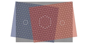
Image Caption: A graphene layer (black) of hexagonally arranged carbon atoms is placed between two layers of boron nitride atoms, which are also arranged hexagonally with a slightly different size. The overlap creates honeycomb patterns in various sizes. (Image: Swiss Nanoscience Institute, University of Basel).
Last year, researchers in the US caused a big stir when they showed that rotating two stacked graphene layers by a “magical” angle of 1.1 degrees turns graphene superconducting—a striking example of how the combination of atomically thin materials can produce completely new electrical properties.
Precision Alignment
Scientists from the Swiss Nanoscience Institute and the Department of Physics at the University of Basel have now taken this concept one step further. They placed a layer of graphene between two boron nitride layers, which is often serves to protect the sensitive carbon structure. Doing so, they aligned the layers very precisely with the crystal lattice of the graphene.
The effect observed by the physicists in Professor Christian Schönenberger’s team is commonly known as a moiré pattern: when two regular patterns are superimposed, a new pattern results with a larger periodic lattice.
New Three-Layer Superlattice
Lujun Wang, a member of the SNI PhD School and researcher in Schönenberger’s team, also observed effects of this kind of superlattice when he combined layers of boron nitride and graphene. The atoms are arranged hexagonally in all layers. If they are stacked on top of each other, larger regular patterns emerge, with a size depending on the angle between the layers.
It had already been shown that this works with a two-layer combination of graphene and boron nitride, but the effects due to a second boron nitride layer had not yet been found.
When the physicists from Basel experimented with three layers, two superlattices were formed between the graphene and the upper and the lower boron nitride layer, respectively. The superposition of all three layers created an even larger superstructure than possible with only one layer.
Scientists are very interested in these types of synthetic materials, since the different moiré patterns can be used to change or artificially produce new electronic material properties.
“To put it simply, the atomic patterns determine the behavior of electrons in a material, and we are combining different naturally occurring patterns to create new synthetic materials,” explains Dr. Andreas Baumgartner, who supervised the project. “Now we have discovered effects in these tailor-made electronic devices that are consistent with a three-layer superstructure,” he adds.
Share on:


Testimonial
"We’re proud to call I-Connect007 a trusted partner. Their innovative approach and industry insight made our podcast collaboration a success by connecting us with the right audience and delivering real results."
Julia McCaffrey - NCAB GroupSuggested Items
Sealed for Survival: Potting Electronics for the Toughest Environments
10/29/2025 | Beth Massey, MacDermid Alpha Electronics SolutionsElectronics deployed in harsh conditions face relentless threats from vibration, impact, chemical contaminants, airborne pollutants, and moisture, conditions that can quickly lead to failure without robust protection. Potting, the process of encapsulating electronics in a protective polymer, is a widely used strategy to safeguard devices from both environmental and mechanical hazards.
Driving Innovation: Mechanical and Optical Processes During Rigid-flex Production
10/28/2025 | Kurt Palmer -- Column: Driving InnovationRigid-flex printed circuit boards are a highly effective solution for placing complex circuitry in tight, three-dimensional spaces. They are now indispensable across a range of industries, from medical devices and aerospace to advanced consumer electronics, helping designers make the most efficient use of available space. However, their unique construction—combining rigid and flexible materials—presents a fundamental challenge for PCB manufacturers.
SMTAI 2025 Review: Reflecting on a Pragmatic and Forward-looking Industry
10/27/2025 | Marcy LaRont, I-Connect007Leaving the show floor on the final afternoon of SMTA International last week in Rosemont, Illinois, it was clear that the show remains a grounded, technically driven event that delivers a solid program, good networking, and an easy space to commune with industry colleagues and meet with customers.
ITW EAE Despatch Ovens Now Support ASTM 5423 Testing
10/15/2025 | ITW EAEAs the demand for high-performance electrical insulation materials continues to grow—driven by the rapid expansion of electric vehicles (EVs) and energy storage systems—thermal processing has become a critical step in material development.
Beyond Thermal Conductivity: Exploring Polymer-based TIM Strategies for High-power-density Electronics
10/13/2025 | Padmanabha Shakthivelu and Nico Bruijnis, MacDermid Alpha Electronics SolutionsAs power density and thermal loads continue to increase, effective thermal management becomes increasingly important. Rapid and efficient heat transfer from power semiconductor chip packages is essential for achieving optimal performance and ensuring long-term reliability of temperature-sensitive components. This is particularly crucial in power systems that support advanced applications such as green energy generation, electric vehicles, aerospace, and defense, along with high-speed computing for data centers and artificial intelligence (AI).