


 Dan’s Biz Bookshelf: ‘Abundance: How We Build a Better Future’
 Trouble in Your Tank: In Complex Systems, Design Rules Aren’t Optional
 It’s Only Common Sense: The Phone Is Still Your Competitive Advantage


Energy-efficient Superconducting Cable for Future Technologies
March 21, 2019 | KITEstimated reading time: 2 minutes
For connecting wind parks, for DC supply on ships, or for lightweight and compact high-current cabling in future electric airplanes: scientists of Karlsruhe Institute of Technology (KIT) have developed a versatile superconducting cable that can be manufactured easily. In case of moderate cooling, it transports electric energy with hardly any losses.
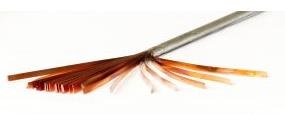
Superconductors transport electrical current at low temperatures with hardly any losses – this makes them attractive for a number of energy-efficient technologies. Usually, however, they require cooling with liquid helium to a temperature near minus 269 degrees Celsius. A new cable made by KIT, the High-temperature Superconductor Cross Conductor (HTS CroCo) can be used at minus 196 degrees Celsius already. “This is due to the special material we use,” say Dr. Walter Fietz and Dr. Michael Wolf of KIT’s Institute for Technical Physics (ITEP). The material is rare-earth barium-copper oxide (REBCO for short), whose superconductivity has been known since 1987. However, long lengths of the superconductor can only be manufactured in the form of thin tapes. “We have developed a method where several REBCO tapes are arranged such that they form a cross. The resulting cable can transport very high currents,” Fietz says.
The HTS CroCo has a higher current-carrying capacity, but needs less space and has a smaller weight than conventional copper or aluminum cables. Manufacture of the cable also is highly efficient. The innovative manufacturing process developed by KIT combines several steps. “Currently, we reach a production speed of one meter per minute on the demonstration scale,” Wolf says. At an accordingly scaled industrial facility, cable lengths of several hundred meters and more might be feasible, which will reduce costs. As the superconducting layer carrying the high current measures only a few thousandths of a millimeter, material expenses are kept within reasonable limits. ”Mass production still is prevented by the high costs for the complex manufacture of REBCO tapes,” Wolf says, “but industry is already developing new processes to reduce costs.”
CroCo is suited for energy-efficient generation of high magnetic fields and for transporting large amounts of electric energy. In future, these cables might be used to integrate large wind parks or solar power plants into the grid and to design leaner “electricity highways”. If liquid hydrogen is used for cooling, CroCo can even transport chemical and electrical energy together. “In principle, a CroCo can be applied wherever space is limited, but the amount of electrical energy to be transported is high,” Fietz says. Hence, application in ships and even in future electric airplanes is feasible.
Being “The Research University in the Helmholtz Association“, KIT creates and imparts knowledge for the society and the environment. It is the objective to make significant contributions to the global challenges in the fields of energy, mobility and information. For this, about 9,300 employees cooperate in a broad range of disciplines in natural sciences, engineering sciences, economics, and the humanities and social sciences. KIT prepares its 25,100 students for responsible tasks in society, industry, and science by offering research-based study programs. Innovation efforts at KIT build a bridge between important scientific findings and their application for the benefit of society, economic prosperity, and the preservation of our natural basis of life.
Share on:


Subscribe
Stay ahead of the technologies shaping the future of electronics with our latest newsletter, Advanced Electronics Packaging Digest. Get expert insights on advanced packaging, materials, and system-level innovation, delivered straight to your inbox.
Subscribe now to stay informed, competitive, and connected.
Suggested Items
Driving Innovation: Selecting the Right Laser Source
04/28/2026 | Simon Khesin -- Column: Driving InnovationWhen I first joined Schmoll Maschinen, I brought experience from almost every PCB process, except for laser. As I immersed myself in laser processing, I realized why it can seem so daunting to a newcomer. The complexity arises from three intersecting factors: A vast variety of laser sources: CO2, UV-nano, green-pico, UV-pico, IR-pico, and others; a diverse range of applications: Drilling, cutting, ablation, and more; and an extensive list of materials: These have vastly different absorption rates. Choosing the right machine or laser source is rarely trivial. Even for experienced engineers, answering "Which source is best?" requires examining the business's specific goals.
Institute of Circuit Technology Spring Seminar 2026: A Bright Future in Europe
04/23/2026 | Pete Starkey, I-Connect007Through the leafy lanes and spring flowers of Warwickshire and back to Meridan, the traditional centre of England, and now officially part of the Metropolitan Borough of Solihull in the county of the West Midlands, I attended the Annual General Meeting and Spring Seminar of the Institute of Circuit Technology (ICT) on April 14. Out of the AGM came notable changes in leadership at the top of the Institute: the retirement of Mat Beadel as chair and Emma Hudson as technical director. Effective May 1, Steve Driver is the new chair, and Alun Morgan is the new technical director.
ACCM Unveils Negative and Near-zero CTE Materials for Large-Format AI Chips
04/21/2026 | Advanced Chip and Circuit MaterialsAdvanced Chip and Circuit Materials, Inc. (ACCM) has launched two new materials: Celeritas HM50, with a negative coefficient of thermal expansion (CTE) of -8 ppm/°C to offset the positive CTE and expansion of copper with temperature on circuit boards, and Celeritas HM001, with near-zero CTE and the low-loss performance needed for high-speed signal layers to 224 Gb/s and faster in artificial intelligence (AI) circuits.
Fresh PCB Concepts: Designing PCBs for Harsh Environments—Reliability Is Engineered Upstream
04/23/2026 | Team NCAB -- Column: Fresh PCB ConceptsWhen engineers hear the phrase “harsh environment,” they usually think of the extreme temperature swings, vibration and shock, pressure changes, or radiation in aerospace. However, aerospace is not the only harsh environment where electronic assemblies must survive. Automotive power electronics, downhole oil and gas tools, marine controls, rail systems, defense platforms, and industrial automation equipment all expose PCBs to environments that are equally unforgiving. The stress mechanisms may differ, but the physics does not.
Advanced Packaging for AI: Reliability Starts at the Cu/Cu/Cu Microvia Junction
04/20/2026 | Kuldip Johal, MKS' AtotechThe rapid growth of AI computing, from training clusters to inference at scale, is reshaping demand across the entire electronics supply chain. Advances in technology requirements, such as higher bandwidth, lower latency, and greater compute density, are driving the development of advanced packaging technologies and transforming the PCB industry across design, manufacturing, testing, and even architecture.