


 Dan’s Biz Bookshelf: ‘Abundance: How We Build a Better Future’
 Trouble in Your Tank: In Complex Systems, Design Rules Aren’t Optional
 It’s Only Common Sense: The Phone Is Still Your Competitive Advantage


NIST Researchers Boost Intensity of Nanowire LEDs
March 21, 2019 | NISTEstimated reading time: 2 minutes
Nanowire gurus at the National Institute of Standards and Technology (NIST) have made ultraviolet light-emitting diodes (LEDs) that, thanks to a special type of shell, produce five times higher light intensity than do comparable LEDs based on a simpler shell design.
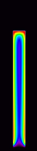
Image Caption: Model of nanowire-based light-emitting diode showing that adding a bit of aluminum to the shell layer (black) directs all recombination of electrons and holes (spaces for electrons) into the nanowire core (multicolored region), producing intense light.
Ultraviolet LEDs are used in a growing number of applications such as polymer curing, water purification and medical disinfection. Micro-LEDs are also of interest for visual displays. NIST staff are experimenting with nanowire-based LEDs for scanning-probe tips intended for electronics and biology applications.
The new, brighter LEDs are an outcome of NIST’s expertise in making high-quality gallium nitride (GaN) nanowires. Lately, researchers have been experimenting with nanowire cores made of silicon-doped GaN, which has extra electrons, surrounded by shells made of magnesium-doped GaN, which has a surplus of “holes” for missing electrons. When an electron and a hole combine, energy is released as light, a process known as electroluminescence.
The NIST group previously demonstrated GaN LEDs that produced light attributed to electrons injected into the shell layer to recombine with holes. The new LEDs have a tiny bit of aluminum added to the shell layer, which reduces losses from electron overflow and light reabsorption.
As described in the journal Nanotechnology, the brighter LEDs are fabricated from nanowires with a so-called “p-i-n” structure, a tri-layer design that injects electrons and holes into the nanowire. The addition of aluminum to the shell helps confine electrons to the nanowire core, boosting the electroluminescence fivefold.
“The role of the aluminum is to introduce an asymmetry in the electrical current that prevents electrons from flowing into the shell layer, which would reduce efficiency, and instead confines electrons and holes to the nanowire core,” first author Matt Brubaker said.
The nanowire test structures were about 440 nanometers (nm) long with a shell thickness of about 40 nm. The final LEDs, including the shells, were almost 10 times larger. Researchers found that the amount of aluminum incorporated into fabricated structures depends on nanowire diameter.
Group leader Kris Bertness said at least two companies are developing micro-LEDs based on nanowires, and NIST has a Cooperative Research and Development Agreement with one of them to develop dopant and structural characterization methods. The researchers have had preliminary discussions with scanning-probe companies about using NIST LEDs in their probe tips, and NIST plans to demonstrate prototype LED tools soon.
The NIST team holds U.S. Patent 8,484,756 on an instrument that combines microwave scanning probe microscopy with an LED for nondestructive, contactless testing of material quality for important semiconductor nanostructures such as transistor channels and individual grains in solar cells. The probe could also be used for biological research on protein unfolding and cell structure.
Share on:


Subscribe
Stay ahead of the technologies shaping the future of electronics with our latest newsletter, Advanced Electronics Packaging Digest. Get expert insights on advanced packaging, materials, and system-level innovation, delivered straight to your inbox.
Subscribe now to stay informed, competitive, and connected.
Suggested Items
OKI Develops 180-Layer, 15 mm PCB for AI Semiconductor Test Equipment
04/29/2026 | BUSINESS WIREOKI Circuit Technology, the OKI Group’s printed circuit board (PCB) business company, has successfully developed design and production technologies for 180-layer, 15 mm-thick PCBs intended for use in wafer testing equipment for high bandwidth memory (HBM) mounted on AI semiconductors.
Target Condition: An Exploration of Flooding PCB Layers
04/02/2026 | Kelly Dack -- Column: Target ConditionThe concept of flooding PCB layers with copper has been around for so long, you’d think we’d have it mastered. We haven’t. (Oh, and by “we,” I mean design engineers and the software tools we depend on.) Years ago, PCB artwork was created by hand using light tables, with tape applied to Mylar. Signals were slow, traces were relatively wide, and high-current paths were simply “beefed up” with wider copper. Signal integrity wasn’t yet a driving concern. Today, solid return paths are fundamental to robust design. We understand the importance of continuous reference planes for signal integrity and EMI control.
Happy’s Tech Talk #47: Automation for Complex Multilayer Fabrication Stackups
03/31/2026 | Happy Holden -- Column: Happy’s Tech TalkMultilayer stackups have evolved dramatically as they’ve been adopted for high-performance computing (HPC) and artificial intelligence (AI) server applications. These high-speed, high I/O designs require the designer and fabricator to manage more boundary conditions than ever before. In practice, the stackup is no longer “just a stackup.” It becomes the foundation for signal integrity, reliability, manufacturability, and cost.
SCHMID Group Wins Major Order for Wet-Process Equipment for AI & HPC Infrastructure
03/11/2026 | SCHMID GroupSCHMID Group, a leading global supplier of advanced wet process equipment for the electronics manufacturing industry, has secured a lower two-digit million-USD purchase order from a major Asian high-end PCB manufacturer for a new HDI multilayer production line.
Standard of Excellence: Building the Board of the Future—Materials, Methods, and Mindset
02/18/2026 | Anaya Vardya -- Column: Standard of ExcellenceThe future of PCB manufacturing is here. The products we’re being asked to build today would have been called “advanced” just a few years ago. What was once special is now standard, and what was once impossible is now expected. The challenge and the opportunity lie in leading the charge to the next frontier of printed circuit board design, materials, and manufacturing discipline. To build the board of the future, we need new materials, smarter methods, and a mindset of innovation anchored in flawless execution.