


 Global PCB Connections: Rigid-flex and Flexible PCBs—The Backbone of Modern Electronics
 Flexible Thinking: The Key to a Successful Flex Circuit Design Transfer
 Happy’s Tech Talk #29: Bend-to-Install Semi-flex FR-4


AT&S Demonstrates Efficiency and Robustness of Embedded Power Technology
April 5, 2019 | AT&SEstimated reading time: 3 minutes
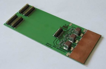
To improve the efficiency in modern cars on the way to electromobility and in challenging industrial power conversion applications the power density has to be increased without limitations on performance and reliability. Based on the AT&S ECP (Embedded Components Packaging) technology, active and passive components have been integrated into PCBs for low-power designs and are used in volume production meeting high-quality requirements. Against this background, the implementation of power semiconductors like MOSFETs or diodes directly into the PCB is a very promising approach to fulfill the increasing needs of electromobility and industrial applications. AT&S successfully used the expertise with its ECP technology for the implementation of efficient power packages and modules. Compared to SMT-based technology a space reduction for the power module of 50% could be realized. In addition, very good results in terms of switching behavior, heat removal and power cycling robustness were achieved.
The EmPower Project
The EUREKA CATRENE “EmPower” project, with the goal to develop a technology for embedded power components for electrical vehicle applications, was running from May 2013 to February 2017. The project was coordinated by AT&S and included ST Microelectronics, Atotech, ILFA, Continental, TU Wien and TU Berlin as further members.
Interconnections between the power devices and wire bonds on direct copper bonded (DCB) substrates are a primary source of parasitic inductances in today’s power packages, leading to significant switching losses, limited lifetime and reliability issues due to the high-power loss density. In contrast, the EmPower embedding concept contains copper interconnections with large cross sections between the power devices and the chip pads by short copper-filled via and large copper cross section. This technology allows the placement of the necessary copper connections and pads on both sides of the package in an arbitrary manner, thus satisfying the needs for both, high electrical and high thermal conductivities. On the other hand, the concept sees the power semiconductors being coated on both sides with copper and embedded in a printed circuit board construction using a galvanic interconnection process. Lastly, making the shortest possible electrical connections between the power semiconductors is minimizing the parasitic inductances and significantly improving the switching performance.
At the heart of the EmPower implementation are so-called power cores as function blocks for power modules. The innovation in terms of the new power concept entails the embedding of power devices such as MOSFETs and diodes as chips with significantly reduced thicknesses in comparison to SMT devices. Cost-effective and effective thermal management is realized by embedding the power semiconductors in a module enabling double sided cooling. This technology allows power semiconductors to be embedded in such a way that the rear of the power module provides a complete copper surface for the connection and allows chips of up to 10 mm x 10 mm to be embedded. The contacting of the pads on the upper side of the components is done by means of micro-via and full area interconnection on the lower side of the devices.
Demonstrators Show High Robustness and Electrical Performance
In order to evaluate the scalability and performance of the new power embedding technology, several demonstrators in the range from 50W to 50kW were developed. The corresponding demonstrators have been realized as a power package (50W, 100V, 20A), a power module (500W, 12-48V, 20A) for a pedelec application and a 50kW power inverter (250V−450V, 200A) for hybrid/electric vehicle applications.
Thermal behavior and electrical performance were investigated successfully with various tests with the 50W and 500W demonstrators in comparison to a standard SMT power package solution as benchmark.
Active power cycling is another important test for power electronic components and modules. Tests with the 500W demonstrator passed more than 300.000 cycles. Other projects with various temperature conditions and stress types show the successful pass of 600.000 cycles and more.
To summarize the outcome of the Embedded Power Project, the concept has shown high potentials according miniaturization, switching performance and thermal management. Reliability according AEC-Q101 have been shown with different tests like power cycling. The technology promises high robustness for power embedding application.
Share on:


Testimonial
"The I-Connect007 team is outstanding—kind, responsive, and a true marketing partner. Their design team created fresh, eye-catching ads, and their editorial support polished our content to let our brand shine. Thank you all! "
Sweeney Ng - CEE PCBSuggested Items
Closing the Loop on PCB Etching Waste
09/09/2025 | Shawn Stone, IECAs the PCB industry continues its push toward greener, more cost-efficient operations, Sigma Engineering’s Mecer System offers a comprehensive solution to two of the industry’s most persistent pain points: etchant consumption and rinse water waste. Designed as a modular, fully automated platform, the Mecer System regenerates spent copper etchants—both alkaline and acidic—and simultaneously recycles rinse water, transforming a traditionally linear chemical process into a closed-loop system.
Driving Innovation: Depth Routing Processes—Achieving Unparalleled Precision in Complex PCBs
09/08/2025 | Kurt Palmer -- Column: Driving InnovationIn PCB manufacturing, the demand for increasingly complex and miniaturized designs continually pushes the boundaries of traditional fabrication methods, including depth routing. Success in these applications demands not only on robust machinery but also sophisticated control functions. PCB manufacturers rely on advanced machine features and process methodologies to meet their precise depth routing goals. Here, I’ll explore some crucial functions that empower manufacturers to master complex depth routing challenges.
Trouble in Your Tank: Minimizing Small-via Defects for High-reliability PCBs
08/27/2025 | Michael Carano -- Column: Trouble in Your TankTo quote the comedian Stephen Wright, “If at first you don’t succeed, then skydiving is not for you.” That can be the battle cry when you find that only small-diameter vias are exhibiting voids. Why are small holes more prone to voids than larger vias when processed through electroless copper? There are several reasons.
The Government Circuit: Navigating New Trade Headwinds and New Partnerships
08/25/2025 | Chris Mitchell -- Column: The Government CircuitAs global trade winds continue to howl, the electronics manufacturing industry finds itself at a critical juncture. After months of warnings, the U.S. Government has implemented a broad array of tariff increases, with fresh duties hitting copper-based products, semiconductors, and imports from many nations. On the positive side, tentative trade agreements with Europe, China, Japan, and other nations are providing at least some clarity and counterbalance.
How Good Design Enables Sustainable PCBs
08/21/2025 | Gerry Partida, Summit InterconnectSustainability has become a key focus for PCB companies seeking to reduce waste, conserve energy, and optimize resources. While many discussions on sustainability center around materials or energy-efficient processes, PCB design is an often overlooked factor that lies at the heart of manufacturing. Good design practices, especially those based on established IPC standards, play a central role in enabling sustainable PCB production. By ensuring designs are manufacturable and reliable, engineers can significantly reduce the environmental impact of their products.