


 Dan’s Biz Bookshelf: ‘Abundance: How We Build a Better Future’
 Trouble in Your Tank: In Complex Systems, Design Rules Aren’t Optional
 It’s Only Common Sense: The Phone Is Still Your Competitive Advantage


Squeezed Nanocrystals
April 8, 2019 | Ames LaboratoryEstimated reading time: 3 minutes
In a collaboration between the U.S. Department of Energy’s Ames Laboratory and Northeastern University, scientists have developed a model for predicting the shape of metal nanocrystals or “islands” sandwiched between or below two-dimensional (2D) materials such as graphene. The advance moves 2D quantum materials a step closer to applications in electronics.
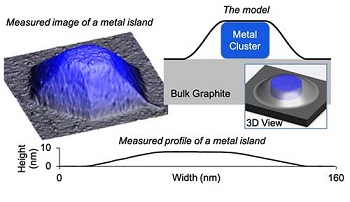
Image Caption: Ames Laboratory and Northeastern University developed and validated a model that predicts the shape of metal nanoparticles blanketed by 2D material. The top blanket of graphene resists deformation, "squeezing" downward on the metal nanoparticle and forcing it to be extremely low and wide.
Ames Laboratory scientist are experts in 2D materials, and recently discovered a first-of-its-kind copper and graphite combination, produced by depositing copper on ion-bombarded graphite at high temperature and in an ultra-high vacuum environment. This produced a distribution of copper islands, embedded under an ultra-thin “blanket” consisting of a few layers of graphene.
“Because these metal islands can potentially serve as electrical contacts or heat sinks in electronic applications, their shape and how they reach that shape are important pieces of information in controlling the design and synthesis of these materials,” said Pat Thiel, an Ames Laboratory scientist and Distinguished Professor of Chemistry and Materials Science and Engineering at Iowa State University.
Ames Laboratory and Northeastern University developed and validated a model that predicts the shape of metal nanoparticles blanketed by 2D material. The top blanket of graphene resists deformation, "squeezing" downward on the metal nanoparticle and forcing it to be extremely low and wide.
Ames Laboratory scientists used scanning tunneling microscopy to painstakingly measure the shapes of more than a hundred nanometer-scale copper islands. This provided the experimental basis for a theoretical model developed jointly by researchers at Northeastern University’s Department of Mechanical and Industrial Engineering and at Ames Laboratory. The model served to explain the data extremely well. The one exception, concerning copper islands less than 10 nm tall, will be the basis for further research.
“We love to see our physics applied, and this was a beautiful way to apply it,” said Scott E. Julien, Ph.D. candidate, at Northeastern. “We were able to model the elastic response of the graphene as it drapes over the copper islands, and use it to predict the shapes of the islands.”
The work showed that the top layer of graphene resists the upward pressure exerted by the growing metal island. In effect, the graphene layer squeezes downward and flattens the copper islands. Accounting for these effects as well as other key energetics leads to the unanticipated prediction of a universal, or size-independent, shape of the islands, at least for sufficiently-large islands of a given metal.
“This principle should work with other metals and other layered materials as well,” said Research Assistant, Ann Lii-Rosales. “Experimentally we want to see if we can use the same recipe to synthesize metals under other types of layered materials with predictable results.”
The research is further discussed in the paper, “Squeezed Nanocrystals: Equilibrium Configuration of Metal Clusters Embedded Beneath the Surface of a Layered Material,” authored by Scott E. Julien, Ann Lii-Rosales, Kai-Tak Wan, Yong Han, Michael C. Tringides, James W. Evans, and Patricia A. Thiel; and published in Nanoscale.
The research was a collaboration between Ames Laboratory and Northeastern University.
Work at Northeastern University was supported by the National Institute of Standards and Technology (NIST), a national facility operated under the U.S. Department of Commerce.
Work at Ames Laboratory was supported primarily by the U.S. Department of Energy Office of Science. This work was also supported in part by a grant of computer time at the National Energy Research Scientific Computing Centre (NERSC), a DOE Office of Science User Facility.
Ames Laboratory is a U.S. Department of Energy Office of Science national laboratory operated by Iowa State University. Ames Laboratory creates innovative materials, technologies and energy solutions. We use our expertise, unique capabilities and interdisciplinary collaborations to solve global problems.
DOE’s Office of Science is the single largest supporter of basic research in the physical sciences in the United States, and is working to address some of the most pressing challenges of our time.
Share on:


Subscribe
Stay ahead of the technologies shaping the future of electronics with our latest newsletter, Advanced Electronics Packaging Digest. Get expert insights on advanced packaging, materials, and system-level innovation, delivered straight to your inbox.
Subscribe now to stay informed, competitive, and connected.
Suggested Items
Driving Innovation: Selecting the Right Laser Source
04/28/2026 | Simon Khesin -- Column: Driving InnovationWhen I first joined Schmoll Maschinen, I brought experience from almost every PCB process, except for laser. As I immersed myself in laser processing, I realized why it can seem so daunting to a newcomer. The complexity arises from three intersecting factors: A vast variety of laser sources: CO2, UV-nano, green-pico, UV-pico, IR-pico, and others; a diverse range of applications: Drilling, cutting, ablation, and more; and an extensive list of materials: These have vastly different absorption rates. Choosing the right machine or laser source is rarely trivial. Even for experienced engineers, answering "Which source is best?" requires examining the business's specific goals.
Institute of Circuit Technology Spring Seminar 2026: A Bright Future in Europe
04/23/2026 | Pete Starkey, I-Connect007Through the leafy lanes and spring flowers of Warwickshire and back to Meridan, the traditional centre of England, and now officially part of the Metropolitan Borough of Solihull in the county of the West Midlands, I attended the Annual General Meeting and Spring Seminar of the Institute of Circuit Technology (ICT) on April 14. Out of the AGM came notable changes in leadership at the top of the Institute: the retirement of Mat Beadel as chair and Emma Hudson as technical director. Effective May 1, Steve Driver is the new chair, and Alun Morgan is the new technical director.
ACCM Unveils Negative and Near-zero CTE Materials for Large-Format AI Chips
04/21/2026 | Advanced Chip and Circuit MaterialsAdvanced Chip and Circuit Materials, Inc. (ACCM) has launched two new materials: Celeritas HM50, with a negative coefficient of thermal expansion (CTE) of -8 ppm/°C to offset the positive CTE and expansion of copper with temperature on circuit boards, and Celeritas HM001, with near-zero CTE and the low-loss performance needed for high-speed signal layers to 224 Gb/s and faster in artificial intelligence (AI) circuits.
Fresh PCB Concepts: Designing PCBs for Harsh Environments—Reliability Is Engineered Upstream
04/23/2026 | Team NCAB -- Column: Fresh PCB ConceptsWhen engineers hear the phrase “harsh environment,” they usually think of the extreme temperature swings, vibration and shock, pressure changes, or radiation in aerospace. However, aerospace is not the only harsh environment where electronic assemblies must survive. Automotive power electronics, downhole oil and gas tools, marine controls, rail systems, defense platforms, and industrial automation equipment all expose PCBs to environments that are equally unforgiving. The stress mechanisms may differ, but the physics does not.
Advanced Packaging for AI: Reliability Starts at the Cu/Cu/Cu Microvia Junction
04/20/2026 | Kuldip Johal, MKS' AtotechThe rapid growth of AI computing, from training clusters to inference at scale, is reshaping demand across the entire electronics supply chain. Advances in technology requirements, such as higher bandwidth, lower latency, and greater compute density, are driving the development of advanced packaging technologies and transforming the PCB industry across design, manufacturing, testing, and even architecture.