


 The Chemical Connection: Onshoring PCB Production—Daunting but Certainly Possible
 It’s Only Common Sense: The Phone Is Still Mightier Than the Keyboard


Laser Processing Method to Increase Efficiency of Optoelectronic Devices
April 15, 2019 | NRLEstimated reading time: 2 minutes
Scientists at the U.S. Naval Research Laboratory (NRL) discovered a new method to passivate defects in next generation optical materials to improve optical quality and enable the miniaturization of light emitting diodes and other optical elements.
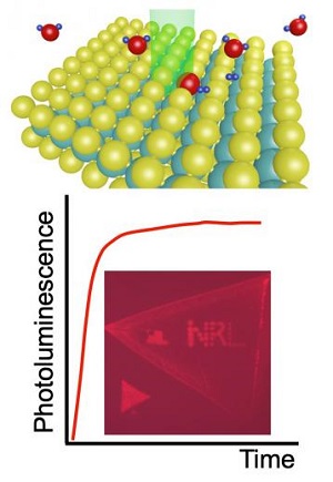
Image Caption: (Top) Illustration of a water molecule bonding at a sulfur vacancy in the MoS2 upon laser light exposure. (Bottom) Photoluminescence (PL) increase observed during laser light exposure in ambient. (Inset) Fluorescence image showing brightened regions spelling out “NRL.” (U.S. Naval Research Laboratory)
“From a chemistry standpoint, we have discovered a new photocatalytic reaction using laser light and water molecules, which is new and exciting,” said Saujan Sivaram, Ph.D., lead author of the study. “From a general perspective, this work enables the integration of high quality, optically active, atomically thin material in a variety of applications, such as electronics, electro-catalysts, memory, and quantum computing applications.”
The NRL scientists developed a versatile laser processing technique to significantly improve the optical properties of monolayer molybdenum disulphide (MoS2)—a direct gap semiconductor—with high spatial resolution. Their process produces a 100-fold increase in the material’s optical emission efficiency in the areas “written” with the laser beam.
According to Sivaram, atomically thin layers of transition metal dichalcogenides (TMDs), such as MoS2, are promising components for flexible devices, solar cells, and optoelectronic sensors due to their high optical absorption and direct band gap.
“These semiconducting materials are particularly advantageous in applications where weight and flexibility are a premium,” he said. “Unfortunately, their optical properties are often highly variable and non-uniform making it critical to improve and control the optical properties of these TMD materials to realize reliable high efficiency devices.”
“Defects are often detrimental to the ability of these monolayer semiconductors to emit light,” Sivaram said. “These defects act as non-radiative trap states, producing heat instead of light, therefore, removing or passivating these defects is an important step towards high efficiency optoelectronic devices.”
In a traditional LED, approximately 90% of the device is a heat sink to improve cooling. Reduced defects enable smaller devices to consume less power, which results in a longer operational lifetime for distributed sensors and low-power electronics.
The researchers demonstrated that water molecules passivate the MoS2 only when exposed to laser light with an energy above the band gap of the TMD. The result is an increase in photoluminescence with no spectral shift.
Treated regions maintain a strong light emission compared to the untreated regions that exhibit much a weaker emission. This suggest that the laser light drives a chemical reaction between the ambient gas molecules and the MoS2.
“This is a remarkable achievement,” said Berend Jonker, Ph.D., senior scientist and principal investigator. “The results of this study pave the way for the use of TMD materials critical to the success of optoelectronic devices and relevant to the Department of Defense mission.”
Share on:


Testimonial
"In a year when every marketing dollar mattered, I chose to keep I-Connect007 in our 2025 plan. Their commitment to high-quality, insightful content aligns with Koh Young’s values and helps readers navigate a changing industry. "
Brent Fischthal - Koh YoungSuggested Items
ITW EAE Despatch Ovens Now Support ASTM 5423 Testing
10/15/2025 | ITW EAEAs the demand for high-performance electrical insulation materials continues to grow—driven by the rapid expansion of electric vehicles (EVs) and energy storage systems—thermal processing has become a critical step in material development.
Beyond Thermal Conductivity: Exploring Polymer-based TIM Strategies for High-power-density Electronics
10/13/2025 | Padmanabha Shakthivelu and Nico Bruijnis, MacDermid Alpha Electronics SolutionsAs power density and thermal loads continue to increase, effective thermal management becomes increasingly important. Rapid and efficient heat transfer from power semiconductor chip packages is essential for achieving optimal performance and ensuring long-term reliability of temperature-sensitive components. This is particularly crucial in power systems that support advanced applications such as green energy generation, electric vehicles, aerospace, and defense, along with high-speed computing for data centers and artificial intelligence (AI).
Is Glass Finally Coming of Age?
10/13/2025 | Nolan Johnson, I-Connect007Substrates, by definition, form the base of all electronic devices. Whether discussing silicon wafers for semiconductors, glass-and-epoxy materials in printed circuits, or the base of choice for interposers, all these materials function as substrates. While other substrates have come and gone, silicon and FR-4 have remained the de facto standards for the industry.
Creative Materials to Showcase Innovative Functional Inks for Medical Devices at COMPAMED 2025
10/09/2025 | Creative Materials, Inc.Creative Materials, a leading manufacturer of high-performance functional inks and coatings, is pleased to announce its participation in COMPAMED 2025, taking place November 17–20 in Düsseldorf, Germany.
Jiva Leading the Charge Toward Sustainable Innovation
09/30/2025 | Marcy LaRont, PCB007 MagazineEnvironmental sustainability in business—product circularity—is a high priority these days. “Circularity,” the term meant to replace “recycling,” in its simplest definition, describes a full circle life for electronic products and all their elements. The result is re-use or a near-complete reintroduction of the base materials back into the supply chain, leaving very little left for waste. For what cannot be reused productively, the ultimate hope is to have better, less harmful means of disposal and/or materials that can seamlessly and harmlessly decompose and integrate back into the natural environment. That is where Jiva and Soluboard come in.