


 Global PCB Connections: Rigid-flex and Flexible PCBs—The Backbone of Modern Electronics
 Flexible Thinking: The Key to a Successful Flex Circuit Design Transfer
 Happy’s Tech Talk #29: Bend-to-Install Semi-flex FR-4


Tuning Terahertz Transmission
April 18, 2019 | A*STAREstimated reading time: 3 minutes
The ability to manipulate light on a subwavelength-scale could lead to a revolution in photonic devices such as antennas, solar panels, and even cloaking devices. Nanotechnology advances have made this possible through the development of metasurfaces, materials covered in features smaller than the wavelength of the light.
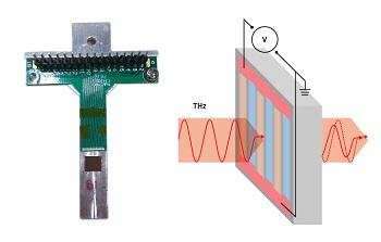
(left) A mounted device including the new tunable metasurface developed by Ding, Teng and co-workers. (right) When terahertz radiation hits the surface of interlinked p-type and n-type semiconducting silicon fingers, the amount of radiation reflected and transmitted can be controlled precisely using an applied voltage.
Now, a team led by A*STAR researchers has produced a highly promising metasurface that can be precisely controlled using a conventional electrical circuit so that it reflects and transmits different amounts of radiation. It can even reach the condition of ‘perfect antireflection’ where it reflects no radiation at all. Specifically, the surface works with broadband terahertz radiation, which is found at the far end of the infrared spectrum and has many potential uses, particularly in security or medical fields.
“Terahertz radiation can penetrate a wide variety of non-conducting materials, but is blocked by liquid water or metals,” explains Lu Ding, who led the work with Jinghua Teng at the A*STAR Institute of Materials Research and Engineering (IMRE). “This means that terahertz beams can be used for material characterization, layer inspection, and producing high-resolution images of the interior of solid objects. It is non-ionizing radiation, and safer than X-rays.”
Previous metasurfaces have been designed to manipulate the reflection of terahertz radiation. However, their application has been limited, as Ding explains: “Conventional terahertz antireflection surfaces are passive and often employ an ultrathin metal coating that, once fabricated, becomes fixed and you can’t actively tune its performance.”
“An electrically tunable metasurface would produce more versatile devices and render more flexibility in system design,” adds Teng. “It is the breakthrough the community is looking for.”
Ding and Teng, along with coworkers at the A*STAR Institute of Microelectronics (IME), Nanyang Technological University, National University of Singapore and Jilin University in China, fabricated their new metasurface on a silicon wafer, using a process entirely compatible with the complementary metal–oxide semiconductor (CMOS) technologies that underpin most electronics.
The exposed metasurface contains stripes of semiconducting silicon, doped with other elements. These stripes are alternately n-type, in which the moving charge carriers are electrons, and p-type, in which the carriers are positively-charged ‘holes’ in the electron structure. When the voltage supplied to the p-n junctions is changed, the reflection and transmission of the radiation also change.
The team realized that the reflection coefficient increased in response to a temperature rise caused by the applied voltage. Meanwhile, the transmission showed a more complex response depending on the voltage polarity, which affected the type of charge carrier that became dominant. Using terahertz time-domain spectroscopy, the team showed that certain voltage conditions caused the echo pulse from the metasurface to vanish, representing complete antireflection.
As well as providing this unprecedented control over reflection and transmission, the metasurface has the benefit of being almost entirely flat at an atomic level. This makes it ideal for building up smooth layers in more complex devices.
“Another big advantage is for our research looking into how 2D materials interact with 2D metamaterials or metasurfaces, a topic in our project in A*STAR’s 2D Semiconductors Pharos Program,” says Teng. “The atomically smooth surface makes the transfer and formation of 2D-Si heterostructures much easier than the patterned surfaces of nano-sized pillars or disks seen on conventional metasurfaces.”
“We could further exploit this type of metasurface by independently biasing the p-n junctions or designing modular functions, meaning that we would have pre-programmable metamaterials,” says Ding. Teng adds that the same platform could be used for studying promising 2D materials like molybdenum disulfide, which exhibits impressive electronic and optical properties for use in new flexible circuits.
Share on:


Testimonial
"The I-Connect007 team is outstanding—kind, responsive, and a true marketing partner. Their design team created fresh, eye-catching ads, and their editorial support polished our content to let our brand shine. Thank you all! "
Sweeney Ng - CEE PCBSuggested Items
Curing and Verification in PCB Shadow Areas
09/17/2025 | Doug Katze, DymaxDesign engineers know a simple truth that often complicates electronics manufacturing: Light doesn’t go around corners. In densely populated PCBs, adhesives and coatings often fail to fully cure in shadowed regions created by tall ICs, connectors, relays, and tight housings.
Marcy’s Musings: Advancing the Advanced Materials Discussion
09/17/2025 | Marcy LaRont -- Column: Marcy's MusingsAs the industry’s most trusted global source of original content about the electronics supply chain, we continually ask you about your concerns, what you care about, and what you most want to learn about. Your responses are insightful and valuable. Thank you for caring enough to provide useful feedback and engage in dialogue.
September 2025 PCB007 Magazine: The Future of Advanced Materials
09/16/2025 | I-Connect007 Editorial TeamMoore’s Law is no more, and the advanced material solutions being developed to grapple with this reality are surprising, stunning, and perhaps a bit daunting. Buckle up for a dive into advanced materials and a glimpse into the next chapters of electronics manufacturing.
I-Connect007 Launches Advanced Electronics Packaging Digest
09/15/2025 | I-Connect007I-Connect007 is pleased to announce the launch of Advanced Electronics Packaging Digest (AEPD), a new monthly digital newsletter dedicated to one of the most critical and rapidly evolving areas of electronics manufacturing: advanced packaging at the interconnect level.
Panasonic Industry will Double the Production Capacity of MEGTRON Multi-layer Circuit Board Materials Over the Next Five Years
09/15/2025 | Panasonic Industry Co., Ltd.Panasonic Industry Co., Ltd., a Panasonic Group company, announced plans for a major expansion of its global production capacity for MEGTRON multi-layer circuit board materials today. The company plans to double its production over the next five years to meet growing demand in the AI server and ICT infrastructure markets.