


 American Made Advocacy: PCBs in the National Spotlight
 Defense Speak Interpreted: Extreme Financial Disparity in Drones and Missiles
 The Right Approach: The End of an Era—DoD Proposes MIL-PRF-31032 Cancellation


An international team of scientists from the National University of Science and Technology “MISIS” (NUST MISIS), Tianjin University (China), as well as from Japan and the United States has developed new energy-efficient iron-based alloys which combine high mechanical and magnetic properties with low cost and open up new opportunities for industry. The research results are published in the Journal of Alloys and Compounds.
Today, scientists from different countries are facing the task of creating new materials which would help to reduce losses in electricity transmission and transformation. This would lead to energy savings and help to reduce emissions of hazardous gases during production (including CO2 — one of the key factors for the greenhouse effect). Electronic devices could be reduced in size by increasing efficiency.
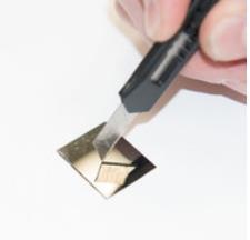
To solve this problem, the international team of scientists engaged in the development of amorphous softmagnetic alloys in low-cost alloy systems such as Fe-Si-B-Nb-Cu (iron-silicon-boron-niobium-copper).
“For the development of new alloys based on iron with a high complex of magnetic and strength properties, we have analyzed a large number of alloy compositions. At the same time, we tried to avoid the use of expensive alloying elements, such as niobium and molybdenum. All the alloys examined in the work were obtained using industrial technology —quenching from a liquid state (melt spinning technic,),” said Andrei Bazlov, one of the authors of the study, an engineer at NUST MISIS.
According to him, the analysis of a large number of Fe82-85B13-16Si1Cu1 alloys allowed scientists to determine the effect of their chemical composition and heat treatment modes on the magnetic and mechanical properties. As a result, they managed to obtain alloys with high magnetic properties, technological plasticity, and ultrahigh strength.
“In terms of their properties, the new amorphous iron-based alloys obtained by us surpass common industrial analogues not only in Russia but also abroad. Their undoubted advantages are relatively low cost (due to the lack of expensive alloying elements) and simplicity of industrial production,” said Andrei Bazlov.
Scientists will continue to develop new compositions and processing regimes of amorphous magnetically soft alloys. They are also planning to implement their developments in the industry.


