


 Global PCB Connections: Rigid-flex and Flexible PCBs—The Backbone of Modern Electronics
 Flexible Thinking: The Key to a Successful Flex Circuit Design Transfer
 Happy’s Tech Talk #29: Bend-to-Install Semi-flex FR-4


Flexible Circuits for 3D Printing
April 29, 2019 | DESYEstimated reading time: 3 minutes
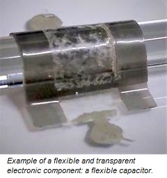
A research cooperation between the University of Hamburg and DESY has developed a process suitable for 3D printing that can be used to produce transparent and mechanically flexible electronic circuits. The electronics consists of a mesh of silver nanowires that can be printed in suspension and embedded in various flexible and transparent plastics (polymers). This technology can enable new applications such as printable light-emitting diodes, solar cells or tools with integrated circuits, as Tomke Glier from the University of Hamburg and her colleagues report in the journal Scientific Reports. The researchers are demonstrating the potential of their process with a flexible capacitor, among other things.
“The aim of this study was to functionalize 3D-printable polymers for different applications,” reports Michael Rübhausen from the Center for Free-Electron Laser Science (CFEL), a cooperation between DESY, the University of Hamburg and the Max Planck Society. “With our novel approach, we want to integrate electronics into existing structural units and improve components in terms of space and weight.” The physics professor from the University of Hamburg led the project together with DESY researcher Stephan Roth, who is also professor at the Royal Institute of Technology in Stockholm. Using the bright X-ray light from DESY's research light source PETRA III and other measuring methods, the team has precisely analyzed the properties of the nanowires in the polymer.
“At the heart of the technology are silver nanowires, which form a conductive mesh,” explains Glier. The silver wires are typically several tens of nanometers (millionths of a millimeter) thick and 10 to 20 micrometers (thousandths of a millimeter) long. The detailed X-ray analysis shows that the structure of the nanowires in the polymer is not changed, but that the conductivity of the mesh even improves thanks to the compression by the polymer, as the polymer contracts during the curing process.
The silver nanowires are applied to a substrate in suspension and dried. “For cost reasons, the aim is to achieve the highest possible conductivity with as few nanowires as possible. This also increases the transparency of the material,” explains Roth, head of the P03 measuring station at DESY's X-ray light source PETRA III, where the X-ray investigations took place. “In this way, layer by layer, a conductive path or surface can be produced.” A flexible polymer is applied to the conductive tracks, which in turn can be covered with conductive tracks and contacts. Depending on the geometry and material used, various electronic components can be printed in this way.
In this paper, the researchers produced a flexible capacitor. “In the laboratory, we carried out the individual work steps in a layering process, but in practice they can later be completely transferred to a 3D printer,” explains Glier. “However, the further development of conventional 3D printing technology, which is usually optimized for individual printing inks, is also essential for this. In inkjet-based processes, the print nozzles could be clogged by the nanostructures,” notes Rübhausen.
In the next step, the researchers now want to test how the structure of the conductive paths made of nanowires changes under mechanical stress. “How well does the wire mesh hold together during bending? How stable does the polymer remain,” said Roth, referring to typical questions. “X-ray investigation is very suitable for this because it is the only way we can look into the material and analyze the conductive paths and surfaces of the nanowires.”
Researchers from the University of Hamburg, the Royal Institute of Technology in Stockholm, the Wallenberg Centre for Wood Science in Stockholm, the Max Planck Institute for the Structure and Dynamics of Matter in Hamburg and DESY were involved in the work.
Share on:


Testimonial
"We’re proud to call I-Connect007 a trusted partner. Their innovative approach and industry insight made our podcast collaboration a success by connecting us with the right audience and delivering real results."
Julia McCaffrey - NCAB GroupSuggested Items
United Electronics Corporation Unveils Revolutionary CIMS Galaxy 30 Automated Optical Inspection System
09/11/2025 | United Electronics CorporationUnited Electronics Corporation (UEC) today announced the launch of its new groundbreaking CIMS Galaxy 30 Automated Optical Inspection (AOI) machine, setting a new industry standard for precision electronics manufacturing quality control. The Galaxy 30, developed and manufactured by CIMS, represents a significant leap forward in inspection technology, delivering exceptional speed improvements and introducing cutting-edge artificial intelligence capabilities.
Intel Announces Key Leadership Appointments to Accelerate Innovation and Strengthen Execution
09/09/2025 | Intel CorporationIntel Corporation today announced a series of senior leadership appointments that support the company’s strategy to strengthen its core product business, build a trusted foundry, and foster a culture of engineering across the business.
DARPA, State of New Mexico Establish Framework to Advance Quantum Computing
09/08/2025 | DARPAAs part of the Quantum Benchmarking Initiative (QBI), DARPA signed an agreement with the State of New Mexico’s Economic Development Department to create the Quantum Frontier Project.
LPKF Strengthens LIDE Technology Leadership with New Patent Protection in Korea
09/04/2025 | LPKFLPKF Laser & Electronics SE today announced that its groundbreaking LIDE (Laser Induced Deep Etching) technology has received additional patent protection in Korea through the Korean Patent Office (KPCA), effective September 1, 2025.
UHDI Fundamentals: UHDI Technology and Industry 4.0
09/03/2025 | Anaya Vardya, American Standard CircuitsUltra high density interconnect (UHDI) technology is rapidly transforming how smart systems are designed and deployed in the context of Industry 4.0. With its capacity to support highly miniaturized, high-performance, and densely packed electronics, UHDI is a critical enabler of the smart, connected, and automated industrial future. Here, I’ll explore the synergy between UHDI and Industry 4.0 technologies, highlighting applications, benefits, and future directions.