


 The Right Approach: Get Ready for ISO 9001 Version 6
 Dan’s Biz Bookshelf: ‘Still Broke: Walmart’s Remarkable Transformation'
 Driving Innovation: Depth Routing Processes—Achieving Unparalleled Precision in Complex PCBs


Candor Builds PCB with Press-Fit Copper Coins, Selective Hard Gold
June 5, 2019 | Candor CircuitsEstimated reading time: 1 minute
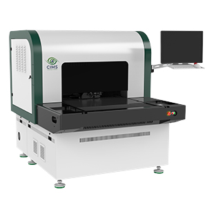
Toronto PCB fabricator, Candor Circuits has built boards with press fitted copper coins and selective hard gold.
Candor is able to press fit and plate over copper coin in the middle of PCB surface areas. This technique allows for thermal management in small profiles. With smaller density parts and higher power, thermal management requires a great deal of experience, know how, and a drive to innovate. Candor’s commitment to producing complex PCB boards quickly has allowed them to excel in thermal management.
Candor’s Technical Sales Manager Sunny Patel commented, “The copper coin selective hard gold plating is a process we can do in faster lead times allowing companies to prototype rapidly with peace of mind.
About Candor Industries
Since 1999, Candor Industries has provided 21st Century customers with innovative PCB solutions for complex technologies through a commitment to service and support. Limitations created by standard manufacturing methods led Candor to invent and develop certain technological advancements, helping them to emerge in the forefront as a top of the line solutions provider. Candor continues to push the envelope of PCB manufacturing through continuous R&D, helping both customers and the industry to a brighter future. For more information about Candor, visit them on the web at www.candorind.com.
Share on:


Testimonial
"In a year when every marketing dollar mattered, I chose to keep I-Connect007 in our 2025 plan. Their commitment to high-quality, insightful content aligns with Koh Young’s values and helps readers navigate a changing industry. "
Brent Fischthal - Koh YoungSuggested Items
Closing the Loop on PCB Etching Waste
09/09/2025 | Shawn Stone, IECAs the PCB industry continues its push toward greener, more cost-efficient operations, Sigma Engineering’s Mecer System offers a comprehensive solution to two of the industry’s most persistent pain points: etchant consumption and rinse water waste. Designed as a modular, fully automated platform, the Mecer System regenerates spent copper etchants—both alkaline and acidic—and simultaneously recycles rinse water, transforming a traditionally linear chemical process into a closed-loop system.
Driving Innovation: Depth Routing Processes—Achieving Unparalleled Precision in Complex PCBs
09/08/2025 | Kurt Palmer -- Column: Driving InnovationIn PCB manufacturing, the demand for increasingly complex and miniaturized designs continually pushes the boundaries of traditional fabrication methods, including depth routing. Success in these applications demands not only on robust machinery but also sophisticated control functions. PCB manufacturers rely on advanced machine features and process methodologies to meet their precise depth routing goals. Here, I’ll explore some crucial functions that empower manufacturers to master complex depth routing challenges.
Trouble in Your Tank: Minimizing Small-via Defects for High-reliability PCBs
08/27/2025 | Michael Carano -- Column: Trouble in Your TankTo quote the comedian Stephen Wright, “If at first you don’t succeed, then skydiving is not for you.” That can be the battle cry when you find that only small-diameter vias are exhibiting voids. Why are small holes more prone to voids than larger vias when processed through electroless copper? There are several reasons.
The Government Circuit: Navigating New Trade Headwinds and New Partnerships
08/25/2025 | Chris Mitchell -- Column: The Government CircuitAs global trade winds continue to howl, the electronics manufacturing industry finds itself at a critical juncture. After months of warnings, the U.S. Government has implemented a broad array of tariff increases, with fresh duties hitting copper-based products, semiconductors, and imports from many nations. On the positive side, tentative trade agreements with Europe, China, Japan, and other nations are providing at least some clarity and counterbalance.
How Good Design Enables Sustainable PCBs
08/21/2025 | Gerry Partida, Summit InterconnectSustainability has become a key focus for PCB companies seeking to reduce waste, conserve energy, and optimize resources. While many discussions on sustainability center around materials or energy-efficient processes, PCB design is an often overlooked factor that lies at the heart of manufacturing. Good design practices, especially those based on established IPC standards, play a central role in enabling sustainable PCB production. By ensuring designs are manufacturable and reliable, engineers can significantly reduce the environmental impact of their products.