


 Global PCB Connections: Rigid-flex and Flexible PCBs—The Backbone of Modern Electronics
 Flexible Thinking: The Key to a Successful Flex Circuit Design Transfer
 Happy’s Tech Talk #29: Bend-to-Install Semi-flex FR-4


Study Contributes to the Production of Flexible Electronic Devices
July 30, 2019 | Agência FAPESPEstimated reading time: 2 minutes
Flexible electronics is one of the most important trends in technology today. The market is growing so fast that it is expected to double in value in the next decade.
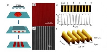
Image Caption: Polythiophene patterning: (a) schematic illustration of the experimental imprinting; (b) confocal microscopy; (c) scanning electron microscopy (SEM) and (d) atomic force microscopy (AFM) micrographs; (e) height profile; (f) 3D view using AFM (image: Scientific Reports).
Extremely light and even bendable optoelectronic equipment that supplies, detects and controls light will become commonplace in the near future. A great deal of research is progressing in this direction, as exemplified by a paper recently published in Scientific Reports.
The paper describes an experimental and theoretical study conducted by Brazilian and Italian researchers to enhance the optical and electronic properties of polythiophene, an electrically conductive and electroluminescent polymer. Organic, light, flexible and easy to process, it is highly attractive in mechanical terms.
“The configuration of polythiophene processed in the most common way, by spin casting, is so disordered as to impair its optical and electronic performance. In our study, we set out to pattern the material in a more ordered manner and make it more selective in emitting and absorbing light,” Marilia Junqueira Caldas told Agência FAPESP. Caldas is a Full Professor at the University of São Paulo’s Physics Institute (IF-USP) in Brazil and participated in the study by contributing to the theoretical framework that described and explained the experimental data.
The pattern she mentioned was obtained via a surprisingly simple stacking arrangement. A droplet of the polymer in solution was deposited on a substrate. As it evaporated, an elastomeric stamp was placed on it to produce a sequence of parallel stripes, which organized the internal structure of the material.
“Patterning made the polymer absorb and emit light in a highly predictable manner, so that stimulated light emission was possible at frequencies not feasible with disordered film. In addition to this gain in selectivity, the resulting device was far lighter than others with a similar function based on stacked layers of several types of semiconductor,” Caldas said.
She explained the relationship between selectivity and ordering as follows. “We calculated its molecular dynamics to find out how it behaved in the disordered phase. We obtained a set of tortuous, intertwined and coupled structures. In this situation, an electron shifted from its initial position by light incidence may become misaligned with the hole left in the atom chain and migrate to distant regions in the interior of the material,” she said.
“This happens to a large number of electrons, and light absorption and emission are highly disordered as a result. Patterning makes the atom chains almost linear, and electrons and holes are very close together in the same chains. The electrons migrate and then return to their starting point, where they emit and absorb light.”
This technique organized the intrinsically disordered material during the process of “growth,” and as such, it can be used in a wide range of optoelectronic applications.
“Our approach demonstrates a viable strategy to direct optical properties through structural control, and the observed optical gain opens up the possibility of using polythiophene nanostructures as building blocks for organic optical amplifiers and active photonic devices,” the authors say in the article.
Caldas and Rodrigo Ramos, whose PhD research she was supervising at the time of the study, received support from FAPESP via the National Science and Technology Institute for Organic Electronics (INEO), one of the National S&T Institutes funded by FAPESP in partnership with Brazil’s National Council for Scientific and Technological Development (CNPq).
Share on:


Testimonial
"Advertising in PCB007 Magazine has been a great way to showcase our bare board testers to the right audience. The I-Connect007 team makes the process smooth and professional. We’re proud to be featured in such a trusted publication."
Klaus Koziol - atgSuggested Items
Dymax Mexico to Showcase Light-Curing Technologies at SMTA Guadalajara Expo & Tech Forum 2025
09/05/2025 | DymaxDymax, a global manufacturer of rapid light-curing materials and equipment, will participate in SMTA Guadalajara Expo & Tech Forum, taking place September 17-18, 2025, at the Guadalajara Expo Center in Guadalajara, Jalisco, Mexico.
September 2025 SMT007 Magazine: An Eye on India
09/02/2025 | I-Connect007 Editorial TeamIndia is on track to become the world’s fastest-growing major economy within the next two years, and that momentum is already reshaping its electronics manufacturing sector. Whether you work with Indian suppliers or serve Indian customers, chances are the country will become a bigger part of your supply chain in the near future.
AiM Future, Franklin Wireless Sign MOU to Jointly Develop Lightweight AI Model and High-Efficiency 1 TOPS AI SoC Chipset
09/01/2025 | BUSINESS WIREAiM Future, a leading AI semiconductor design company, has signed a Memorandum of Understanding (MOU) with Franklin Wireless Corp., a global leader in intelligent wireless solutions, to jointly develop a lightweight AI model and a high-efficiency 1 TOPS performance AI SoC chipset.
Dymax Renews Connecticut Headquarters Lease, Reinforces Long-Term Commitment to Local Community
08/08/2025 | DymaxDymax, a global manufacturer of rapid light-curing materials and equipment, is pleased to announce the renewal and extension of its corporate lease at its 318 Industrial Lane, Torrington, headquarters.
MoU to Revolutionize Photonic Integrated Circuit (PIC) Device Testing with AI-Driven Solutions
08/07/2025 | PRNewswireLightium AG, MPI Corporation, and Axiomatic_AI Inc. have entered into a Memorandum of Understanding (MoU) to jointly develop the world's first Intelligent, Autonomous, and Integrated Test Solution (IAITS) for photonic devices.