


 Dan’s Biz Bookshelf: ‘Abundance: How We Build a Better Future’
 Trouble in Your Tank: In Complex Systems, Design Rules Aren’t Optional
 It’s Only Common Sense: The Phone Is Still Your Competitive Advantage


Novel Process for Structuring Quantum Materials
August 1, 2019 | Forschungszentrum JülichEstimated reading time: 2 minutes
Implementing quantum materials in computer chips provides access to fundamentally new technologies. In order to build powerful and fault-resistant quantum computers, it is possible, for example, to combine topological insulators with superconductors. This process step brings with it some challenges that have now been solved by researchers from Jülich.
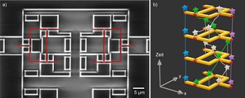
Image Caption: a) Scanning electron micrograph during the "Jülich process": A chip can be seen during fabrication. The topological insulator (dyed red) has already been selectively deposited. In a next fabrication step, the superconductor is applied via shadow mask deposition. In black-and-white, various mask systems are recognizable which make it possible to manufacture the desired components completely in ultrahigh vacuum. b) In such networks one wants to try to move so-called majorana modes (represented as stars) along the topological tracks in order to enable topologically protected quantum computing operations. While the blue and violet Majorana fashion stays in the same position (x, y) in the room. Credit: Forschungszentrum Jülich / Peter Schüffelgen
Even the ancient Inca used knots in cords to encode and store information in their ancient writing "Quipu". The advantage: unlike ink on a sheet of paper, the information stored in the knot is robust against external destructive influences, such as water. Even novel quantum computers should be able to store information robustly in the form of nodes. For this, however, no cord is knotted, but so-called quasi-particles in space and time.
What is needed to build such a quantum node machine are new materials called quantum materials. Experts speak of topological insulators and superconductors. The processing of these materials to components for quantum computers is a challenge in itself; especially because topological insulators are very sensitive to air.
Scientists in Jülich have now developed a novel process that makes it possible to structure quantum materials without exposing them to air during processing. The so-called "Jülich process" makes it possible to combine superconductors and topological insulators in ultrahigh vacuum to produce complex components.
Initial measurements in their samples indicate evidence of majorana states. "Majoranas" are exactly the promising quasiparticles to be knotted in the shown networks of topological insulators and superconductors to enable robust quantum computing. In a next step, the researchers of the Peter Grünberg Institute, together with their colleagues from Aachen, the Netherlands and China, will provide their networks with readout and control electronics in order to make the quantum materials available for the application.
Share on:


Subscribe
Stay ahead of the technologies shaping the future of electronics with our latest newsletter, Advanced Electronics Packaging Digest. Get expert insights on advanced packaging, materials, and system-level innovation, delivered straight to your inbox.
Subscribe now to stay informed, competitive, and connected.
Suggested Items
AI Demand Drives PCB Material Market Growth
05/08/2026 | TPCAAs AI computing continues to drive a comprehensive upgrade in hardware specifications, the global printed circuit board industry is undergoing a profound structural transformation.
I-Connect007 Editor’s Choice: Five Must-Reads for the Week
05/01/2026 | Michelle Te, I-Connect007If it feels like the PCB industry is accelerating faster than ever, you’re not imagining it. From advanced materials driven by AI applications to renewed investment in domestic manufacturing—and the next generation stepping into critical roles—there’s a lot shifting at once. My selections for this week highlight where the pressure points are forming, and where the opportunities are emerging.
Electronics Manufacturing Needs Your Voice: Global Sentiment Survey Now Live
04/30/2026 | Global Electronics AssociationThe latest monthly Global Sentiment Survey from the Global Electronics Association is now open. At a time when demand uncertainty, policy shifts, energy costs, and supply chain recalibration are pulling the industry in multiple directions, the survey captures something macroeconomic data often misses: how manufacturers are actually experiencing conditions on the ground.
From Backbone to Breakthroughs: I-Connect007 Wraps PCB Materials Series with Focus on Innovation
05/06/2026 | I-Connect007I-Connect007 wraps up its six-part podcast series, PCB Materials: The Backbone and Future of Electronics, with Episode 6 and a discussion focusing on innovation. In Episode 6, Marcy LaRont speaks with Isola CTO Kirk Thompson about a critical turning point for the PCB industry as innovation accelerates. As data rates climb and demands from AI infrastructure, power density, flexible electronics, photonics, and chiplet integration intensify, traditional material assumptions are no longer sufficient.
Jiva Soluboard Getting the Attention It Deserves
04/30/2026 | Marcy LaRont, I-Connect007 MagazineJiva is a newer company that bridges the divide between PCB fabrication and product circularity or sustainability. Jiva Soluboard is the first fully recyclable laminate material ever created for PCB fabrication, and it's not going unnoticed. Stephen Driver, CEO of Jiva, gave us an update at APEX EXPO, including an exciting certification achievement in February.