


 Dan’s Biz Bookshelf: ‘Abundance: How We Build a Better Future’
 Trouble in Your Tank: In Complex Systems, Design Rules Aren’t Optional
 It’s Only Common Sense: The Phone Is Still Your Competitive Advantage


Synthesizing Single-Crystalline Hexagonal Graphene Quantum Dots
August 6, 2019 | KAISTEstimated reading time: 2 minutes
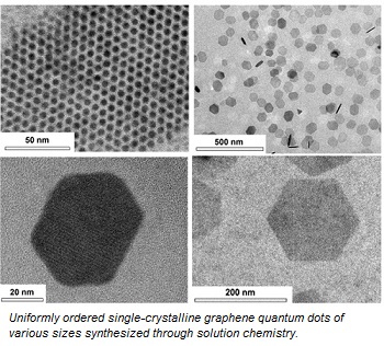
A KAIST team has designed a novel strategy for synthesizing single-crystalline graphene quantum dots, which emit stable blue light. The research team confirmed that a display made of their synthesized graphene quantum dots successfully emitted blue light with stable electric pressure, reportedly resolving the long-standing challenges of blue light emission in manufactured displays. The study, led by Professor O Ok Park in the Department of Chemical and Biological Engineering, was featured online in Nano Letters on July 5.
Graphene has gained increased attention as a next-generation material for its heat and electrical conductivity as well as its transparency. However, single and multi-layered graphene have characteristics of a conductor so that it is difficult to apply into semiconductor. Only when downsized to the nanoscale, semiconductor’s distinct feature of bandgap will be exhibited to emit the light in the graphene. This illuminating featuring of dot is referred to as a graphene quantum dot.
Conventionally, single-crystalline graphene has been fabricated by chemical vapor deposition (CVD) on copper or nickel thin films, or by peeling graphite physically and chemically. However, graphene made via chemical vapor deposition is mainly used for large-surface transparent electrodes. Meanwhile, graphene made by chemical and physical peeling carries uneven size defects.
The research team explained that their graphene quantum dots exhibited a very stable single-phase reaction when they mixed amine and acetic acid with an aqueous solution of glucose. Then, they synthesized single-crystalline graphene quantum dots from the self-assembly of the reaction intermediate. In the course of fabrication, the team developed a new separation method at a low-temperature precipitation, which led to successfully creating a homogeneous nucleation of graphene quantum dots via a single-phase reaction.
Professor Park and his colleagues have developed solution phase synthesis technology that allows for the creation of the desired crystal size for single nanocrystals down to 100 nano meters. It is reportedly the first synthesis of the homogeneous nucleation of graphene through a single-phase reaction.
Professor Park said, "This solution method will significantly contribute to the grafting of graphene in various fields. The application of this new graphene will expand the scope of its applications such as for flexible displays and varistors.”
This research was a joint project with a team from Korea University under Professor Sang Hyuk Im from the Department of Chemical and Biological Engineering, and was supported by the National Research Foundation of Korea, the Nano-Material Technology Development Program from the Electronics and Telecommunications Research Institute (ETRI), KAIST EEWS, and the BK21+ project from the Korean government.
Share on:


Subscribe
Stay ahead of the technologies shaping the future of electronics with our latest newsletter, Advanced Electronics Packaging Digest. Get expert insights on advanced packaging, materials, and system-level innovation, delivered straight to your inbox.
Subscribe now to stay informed, competitive, and connected.
Suggested Items
Driving Innovation: Selecting the Right Laser Source
04/28/2026 | Simon Khesin -- Column: Driving InnovationWhen I first joined Schmoll Maschinen, I brought experience from almost every PCB process, except for laser. As I immersed myself in laser processing, I realized why it can seem so daunting to a newcomer. The complexity arises from three intersecting factors: A vast variety of laser sources: CO2, UV-nano, green-pico, UV-pico, IR-pico, and others; a diverse range of applications: Drilling, cutting, ablation, and more; and an extensive list of materials: These have vastly different absorption rates. Choosing the right machine or laser source is rarely trivial. Even for experienced engineers, answering "Which source is best?" requires examining the business's specific goals.
Institute of Circuit Technology Spring Seminar 2026: A Bright Future in Europe
04/23/2026 | Pete Starkey, I-Connect007Through the leafy lanes and spring flowers of Warwickshire and back to Meridan, the traditional centre of England, and now officially part of the Metropolitan Borough of Solihull in the county of the West Midlands, I attended the Annual General Meeting and Spring Seminar of the Institute of Circuit Technology (ICT) on April 14. Out of the AGM came notable changes in leadership at the top of the Institute: the retirement of Mat Beadel as chair and Emma Hudson as technical director. Effective May 1, Steve Driver is the new chair, and Alun Morgan is the new technical director.
ACCM Unveils Negative and Near-zero CTE Materials for Large-Format AI Chips
04/21/2026 | Advanced Chip and Circuit MaterialsAdvanced Chip and Circuit Materials, Inc. (ACCM) has launched two new materials: Celeritas HM50, with a negative coefficient of thermal expansion (CTE) of -8 ppm/°C to offset the positive CTE and expansion of copper with temperature on circuit boards, and Celeritas HM001, with near-zero CTE and the low-loss performance needed for high-speed signal layers to 224 Gb/s and faster in artificial intelligence (AI) circuits.
Fresh PCB Concepts: Designing PCBs for Harsh Environments—Reliability Is Engineered Upstream
04/23/2026 | Team NCAB -- Column: Fresh PCB ConceptsWhen engineers hear the phrase “harsh environment,” they usually think of the extreme temperature swings, vibration and shock, pressure changes, or radiation in aerospace. However, aerospace is not the only harsh environment where electronic assemblies must survive. Automotive power electronics, downhole oil and gas tools, marine controls, rail systems, defense platforms, and industrial automation equipment all expose PCBs to environments that are equally unforgiving. The stress mechanisms may differ, but the physics does not.
Advanced Packaging for AI: Reliability Starts at the Cu/Cu/Cu Microvia Junction
04/20/2026 | Kuldip Johal, MKS' AtotechThe rapid growth of AI computing, from training clusters to inference at scale, is reshaping demand across the entire electronics supply chain. Advances in technology requirements, such as higher bandwidth, lower latency, and greater compute density, are driving the development of advanced packaging technologies and transforming the PCB industry across design, manufacturing, testing, and even architecture.