


 Dan’s Biz Bookshelf: ‘Abundance: How We Build a Better Future’
 Trouble in Your Tank: In Complex Systems, Design Rules Aren’t Optional
 It’s Only Common Sense: The Phone Is Still Your Competitive Advantage


Quantum Interferometry Demonstrated in Silicon at More Practical Temperatures
August 6, 2019 | RIKENEstimated reading time: 2 minutes
Using a silicon-based transistor similar to those found in everyday electronics, RIKEN researchers have produced a functional quantum ‘qubit’—the quantum equivalent of bits used in conventional computers—that operates above the extremely low temperatures typically needed to observe quantum interference effects.
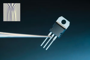
Image Caption: Figure 1: By fabricating a simple three-terminal device that is similar to a general transistor using standard microfabrication techniques, RIKEN researchers could observe quantum interference effects of a single qubit while continuously varying the energy level of the qubit (inset).
The study breaks open the exploration of quantum interference to enable research using standard materials and techniques at more accessible temperatures.
Many highly sensitive measurement techniques are based on monitoring the interference of waves. The most well-known example is the detection of extremely weak gravitational waves generated by colliding neutron stars and black holes using the interference between two laser beams that are several kilometers long. Many scientists are working on extending this technique to the wave functions of quantum objects since this would permit much more sensitive sensing than is possible using classical waves.
A promising system for achieving such quantum interferometry is silicon because researchers can draw on the many decades of research and development that have gone into conventional silicon-based electronics and integrated circuits. In particular, spin qubits in silicon could be used for quantum interferometry, but semiconductor qubits typically need temperatures very close to absolute zero, which necessitates using bulky and expensive cryogenic equipment.
Now, Keiji Ono of the RIKEN Advanced Device Laboratory and his co-workers have raised the operating temperature of qubits in silicon to 1.6 kelvin. “This is in the ‘high temperature’ range, which might sound strange, but compared with the 0.1 kelvin temperatures usually required for semiconductor qubits, these high temperatures can be produced in a less expensive, smaller facility and in a short time,” comments Ono. “This is a major achievement and will reduce the hurdles for any research group trying to enter this area of research and development.”
The researchers fabricated a simple three-terminal device similar to a general transistor using standard microfabrication techniques, and were able to observe the quantum interference effects of the single qubit while continuously varying the energy level of the qubit (inset of Fig. 1).
“I wanted to use a silicon device as a universal basis for exploring ubiquitous, material-independent quantum effects,” explains Ono. “Furthermore, our device is not just a laboratory device made using silicon material, but a practical device that actually forms part of a large-scale integrated circuit.”
The results that the team obtained using the device agreed well with theory. “Our single qubit calculates the weighted average of two input variables using quantum interference,” says Ono. “We achieved almost perfect agreement between the experiments and calculations, confirming the ubiquitous nature of the observed quantum interference effect.”
Share on:


Subscribe
Stay ahead of the technologies shaping the future of electronics with our latest newsletter, Advanced Electronics Packaging Digest. Get expert insights on advanced packaging, materials, and system-level innovation, delivered straight to your inbox.
Subscribe now to stay informed, competitive, and connected.
Suggested Items
STMicroelectronics Enables Always-On Vision with Ultralow-Power Image Sensors
05/01/2026 | STMicroelectronicsSTMicroelectronics, a global semiconductor leader serving customers across the spectrum of electronics applications, introduces a new generation of ultralow-power global-shutter image sensors that deliver high-quality, always-on vision to compact devices operating on batteries or harvested energy.
Alpha, Omega Semiconductor Launches SmartClamp DrMOS for AI Servers and GPUs
05/01/2026 | AlphaAlpha and Omega Semiconductor Limited (AOS) a designer, developer, and global supplier of a broad range of discrete power devices, wide bandgap power devices, power management ICs, and modules, announced the launch of the SmartClamp™ family of protected DrMOS.
Skoltech Team Develops Modulator for Compact Photonic Integrated Circuits
04/28/2026 | SkoltechResearchers at Skoltech have developed an ultra-compact electro-optic modulator based on silicon photonics and plasmonics that enables high-efficiency optical signal control within a small device footprint.
UHDI Fundamentals– Applications, Challenges, and the Future of Flex–Packaging Integration, Part 2
04/16/2026 | Anaya Vardya, American Standard CircuitsIn the second of this two-part series, Anaya Vardya of American Standard Circuits examines applications, challenges, manufacturing considerations, and future trends emerging from the convergence of flexible printed circuit boards and advanced semiconductor packaging. Applications driving the convergence include consumer electronics, automotive systems, medical, wearables, aerospace and more.
BEST Inc. Publishes Optimizing BGA Rework Techniques to Ensure Quality Tech Paper
04/15/2026 | BEST Inc.BEST Inc., a leader in electronic component and PCB services, is pleased to announce they have published a tech paper describing techniques for reworking BGA components to ensure quality during the printed circuit board rework process.