


 Dan’s Biz Bookshelf: ‘Abundance: How We Build a Better Future’
 Trouble in Your Tank: In Complex Systems, Design Rules Aren’t Optional
 It’s Only Common Sense: The Phone Is Still Your Competitive Advantage


Greener, Faster and Cheaper Way to Make Patterned Metals for Solar Cells and Electronics
August 14, 2019 | University of WarwickEstimated reading time: 2 minutes
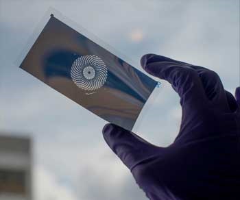
An innovative way to pattern metals has been discovered by scientists in the Department of Chemistry at the University of Warwick, which could make the next generation of solar panels more sustainable and cheaper.
Silver and copper are the most widely used electrical conductors in modern electronics and solar cells. However, conventional methods of patterning these metals to make the desired pattern of conducting lines are based on selectively removing metal from a film by etching using harmful chemicals or printing from costly metal inks.
Scientists from the Department of Chemistry at the University of Warwick, have developed a way of patterning these metals that is likely to prove much more sustainable and cheaper for large scale production, because there is no metal waste or use of toxic chemicals, and the fabrication method is compatible with continuous roll-to-roll processing.
The work is reported in the paper ‘Selective deposition of silver and copper films by condensation coefficient modulation’ published as an advanced article in the journal Materials Horizons ("Selective deposition of silver and copper films by condensation coefficient modulation").
Thanks to £1.15 M funding from the UK Engineering and Physical Sciences Research Council, Dr Ross Hatton and Dr Silvia Varagnolo have discovered that silver and copper do not condense onto extremely thin films of certain highly fluorinated organic compounds when the metal is deposited by simple thermal evaporation.
Thermal evaporation is already widely used on a large scale to make the thin metal film on the inside of crisp packets, and organofluorine compounds are already common place as the basis of non-stick cooking pans.
The researchers have shown that the organofluorine layer need only be 10 billionths of a metre thick to be effective, and so only tiny amounts are needed.
This unconventional approach also leaves the metal surface uncontaminated, which Hatton believes will be particularly important for the next generation sensors, which often require uncontaminated patterned films of these metals as platforms onto which sensing molecules can be attached.
To help address the challenges posed by climate change, there is a need for colour tuneable, flexible and light weight solar cells that can be produced at low cost, particularly for applications where conventional rigid silicon solar cells are unsuitable such as in electric cars and semi-transparent solar cells for buildings.
Solar cells based on thin films of organic, perovskite or nano-crystal semiconductors all have potential to meet this need, although they all require a low cost, flexible transparent electrode. Hatton and his team have used their method to fabricate semi-transparent organic solar cells in which the top silver electrode is patterned with millions of tiny apertures per square centimetre, which cannot be achieved by any other scalable means directly on top of an organic electronic device.
Dr Hatton from the Department of Chemistry at the University of Warwick comments: “This innovation enables us to realise the dream of truly flexible, transparent electrodes matched to needs of the emerging generation of thin film solar cells, as well as having numerous other potential applications ranging from sensors to low-emissivity glass.”
Share on:


Subscribe
Stay ahead of the technologies shaping the future of electronics with our latest newsletter, Advanced Electronics Packaging Digest. Get expert insights on advanced packaging, materials, and system-level innovation, delivered straight to your inbox.
Subscribe now to stay informed, competitive, and connected.
Suggested Items
Driving Innovation: Selecting the Right Laser Source
04/28/2026 | Simon Khesin -- Column: Driving InnovationWhen I first joined Schmoll Maschinen, I brought experience from almost every PCB process, except for laser. As I immersed myself in laser processing, I realized why it can seem so daunting to a newcomer. The complexity arises from three intersecting factors: A vast variety of laser sources: CO2, UV-nano, green-pico, UV-pico, IR-pico, and others; a diverse range of applications: Drilling, cutting, ablation, and more; and an extensive list of materials: These have vastly different absorption rates. Choosing the right machine or laser source is rarely trivial. Even for experienced engineers, answering "Which source is best?" requires examining the business's specific goals.
Institute of Circuit Technology Spring Seminar 2026: A Bright Future in Europe
04/23/2026 | Pete Starkey, I-Connect007Through the leafy lanes and spring flowers of Warwickshire and back to Meridan, the traditional centre of England, and now officially part of the Metropolitan Borough of Solihull in the county of the West Midlands, I attended the Annual General Meeting and Spring Seminar of the Institute of Circuit Technology (ICT) on April 14. Out of the AGM came notable changes in leadership at the top of the Institute: the retirement of Mat Beadel as chair and Emma Hudson as technical director. Effective May 1, Steve Driver is the new chair, and Alun Morgan is the new technical director.
ACCM Unveils Negative and Near-zero CTE Materials for Large-Format AI Chips
04/21/2026 | Advanced Chip and Circuit MaterialsAdvanced Chip and Circuit Materials, Inc. (ACCM) has launched two new materials: Celeritas HM50, with a negative coefficient of thermal expansion (CTE) of -8 ppm/°C to offset the positive CTE and expansion of copper with temperature on circuit boards, and Celeritas HM001, with near-zero CTE and the low-loss performance needed for high-speed signal layers to 224 Gb/s and faster in artificial intelligence (AI) circuits.
Fresh PCB Concepts: Designing PCBs for Harsh Environments—Reliability Is Engineered Upstream
04/23/2026 | Team NCAB -- Column: Fresh PCB ConceptsWhen engineers hear the phrase “harsh environment,” they usually think of the extreme temperature swings, vibration and shock, pressure changes, or radiation in aerospace. However, aerospace is not the only harsh environment where electronic assemblies must survive. Automotive power electronics, downhole oil and gas tools, marine controls, rail systems, defense platforms, and industrial automation equipment all expose PCBs to environments that are equally unforgiving. The stress mechanisms may differ, but the physics does not.
Advanced Packaging for AI: Reliability Starts at the Cu/Cu/Cu Microvia Junction
04/20/2026 | Kuldip Johal, MKS' AtotechThe rapid growth of AI computing, from training clusters to inference at scale, is reshaping demand across the entire electronics supply chain. Advances in technology requirements, such as higher bandwidth, lower latency, and greater compute density, are driving the development of advanced packaging technologies and transforming the PCB industry across design, manufacturing, testing, and even architecture.