


 Global PCB Connections: Rigid-flex and Flexible PCBs—The Backbone of Modern Electronics
 Flexible Thinking: The Key to a Successful Flex Circuit Design Transfer
 Happy’s Tech Talk #29: Bend-to-Install Semi-flex FR-4


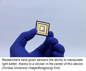
Sticker Makes Nanoscale Light Manipulation Easier to Manufacture
August 26, 2019 | Purdue UniversityEstimated reading time: 1 minute
Human pathogens, such as HIV and viruses causing respiratory tract infection, have molecular fingerprints that are difficult to distinguish. To better detect these pathogens, sensors in diagnostic tools need to manipulate light on a nanoscale.
But there isn’t a good way to manufacture these light manipulation devices without damaging the sensors. Purdue University engineers have a solution: Stickers.
In a paper published in Nano Letters, the team integrated light manipulation devices called 3D plasmonic nanoarrays onto peelable films that can stick to any surface. They tested the sticker-nanoarray’s capabilities on the lenses of sensors, which make up conventional imaging systems.
The Air Force Research Laboratory supported the work and validated the sticker’s performance and properties.
“Unlike any existing approaches, the entire process occurs in distilled water at room temperature without the chemical, thermal or mechanical treatments that can damage sensitive surfaces, such as a sensor lens,” said Chi Hwan Lee, an assistant professor of biomedical engineering and mechanical engineering at Purdue.
To turn the nanoarrays into a sticker, the researchers built them into a film on a silicon wafer. When submerged in distilled water, the film peels cleanly from the wafer, allowing the wafer to be reused. The film can then stick to the desired surface without damaging it.
“Because this methodology allows 3D plasmonic nanoarrays to physically separate from a donor wafer and transfer over to another surface without defect, it offers a major cost- and time-saving factor in the manufacturing scheme,” Lee said.
The researchers also demonstrated that the process works for various classes of 3D plasmonic nanoarrays in both lateral and vertical configurations, offering more functionality.
Lee’s lab plans to further develop these sticker-nanoarrays for biological sensing applications, such as for protein detection in clinical diagnostics. The lab has already created electronic stickers that serve as bio-patches for drug delivery. They also can enable ordinary objects to wirelessly connect to a network, creating an “Internet of Things.”
The method has been patented via the Purdue Research Foundation Office of Technology Commercialization. This research aligns with Purdue's Giant Leaps celebration, acknowledging the university’s global advancements made in health, longevity and quality of life as part of Purdue’s 150th anniversary. This is one of the four themes of the yearlong celebration’s Ideas Festival, designed to showcase Purdue as an intellectual center solving real-world issues.
Share on:


Testimonial
"In a year when every marketing dollar mattered, I chose to keep I-Connect007 in our 2025 plan. Their commitment to high-quality, insightful content aligns with Koh Young’s values and helps readers navigate a changing industry. "
Brent Fischthal - Koh YoungSuggested Items
Driving Innovation: Depth Routing Processes—Achieving Unparalleled Precision in Complex PCBs
09/08/2025 | Kurt Palmer -- Column: Driving InnovationIn PCB manufacturing, the demand for increasingly complex and miniaturized designs continually pushes the boundaries of traditional fabrication methods, including depth routing. Success in these applications demands not only on robust machinery but also sophisticated control functions. PCB manufacturers rely on advanced machine features and process methodologies to meet their precise depth routing goals. Here, I’ll explore some crucial functions that empower manufacturers to master complex depth routing challenges.
Polar Instruments Announces Additive Transmission Line Support for Si9000e
08/20/2025 | Polar InstrumentsTransmission lines embedded into the PCB surface are a feature of UHDI constructions. The 2025 fall release of Polar's Si9000e PCB impedance & insertion loss transmission line field solver incorporates eight new single ended, differential and coplanar transmission line structures.
Henniker Plasma Launches Stratus Turnkey Plasma Manufacturing Cell
08/13/2025 | Henniker PlasmaHenniker Plasma, a leading manufacturer of plasma treatment systems, proudly announces the launch of its Stratus Plasma Manufacturing Cell range — a fully integrated, turnkey solution that combines advanced atmospheric plasma surface treatment with robotic automation.
Trouble in Your Tank: Metallizing Flexible Circuit Materials—Mitigating Deposit Stress
08/04/2025 | Michael Carano -- Column: Trouble in Your TankMetallizing materials, such as polyimide used for flexible circuitry and high-reliability multilayer printed wiring boards, provide a significant challenge for process engineers. Conventional electroless copper systems often require pre-treatments with hazardous chemicals or have a small process window to achieve uniform coverage without blistering. It all boils down to enhancing the adhesion of the thin film of electroless copper to these smooth surfaces.
Designers Notebook: Basic PCB Planning Criteria—Establishing Design Constraints
07/22/2025 | Vern Solberg -- Column: Designer's NotebookPrinted circuit board development flows more smoothly when all critical issues are predefined and understood from the start. As a basic planning strategy, the designer must first consider the product performance criteria, then determine the specific industry standards or specifications that the product must meet. Planning also includes a review of all significant issues that may affect the product’s manufacture, performance, reliability, overall quality, and safety.