


 The Right Approach: Get Ready for ISO 9001 Version 6
 Dan’s Biz Bookshelf: ‘Still Broke: Walmart’s Remarkable Transformation'
 Driving Innovation: Depth Routing Processes—Achieving Unparalleled Precision in Complex PCBs


New Topological Insulator Can Reroute Photonic ‘Traffic’ On the Fly, Making for Faster Chips
September 16, 2019 | PennEngineeringEstimated reading time: 3 minutes
Topological insulators are a game-changing class of materials; charged particles can flow freely on their edges and route themselves around defects, but can’t pass through their interiors. This perfect surface conduction holds promise for fast and efficient electronic circuits, though engineers must contend with the fact that the interiors of such materials are effectively wasted space.
Now, researchers from the University of Pennsylvania, where topological insulators were first discovered in 2005, have shown a way to fulfill that promise in a field where physical space is at an even bigger premium: photonics. They have shown, for the first time, a way for a topological insulator to make use of its entire footprint.
By using photons instead of electrons, photonic chips promise even faster data transfer speeds and information-dense applications, but the components necessary for building them remain considerably larger than their electronic counterparts, due to the lack of efficient data-routing architecture.
A photonic topological insulator with edges that can be redefined on the fly, however, would help solve the footprint problem. Being able to route these “roads” around one another as needed means the entire interior bulk could be used to efficiently build data links.
Researchers at Penn’s School of Engineering and Applied Science have built and tested such a device for the first time, publishing their findings in the journal Science.
“This could have a big impact on large-information capacity applications, like 5G, or even 6G, cellphone networks,” says Liang Feng, assistant professor in Penn Engineering’s Departments of Materials Science and Engineering and Electrical and Systems Engineering.
“We think this may be the first practical application of topological insulators,” he says.
Feng led the study along with graduate student Han Zhao, a member of his lab. Fellow lab members Xingdu Qiao, Tianwei Wu and Bikashkali Midya, along with Stefano Longhi, professor at the Polytechnic University of Milan in Italy, also contributed to the research.
The data centers that form the backbone of communication networks route calls, texts, email attachments and streaming movies to and between millions of cellular devices. But as the amount of data flowing through these data centers increases, so does the need for high-capacity data routing that can keep up with the demand.
Switching from electrons to photons would speed up this process for the upcoming information explosion, but engineers must first design a whole new library of devices for getting those photons from input to output without mixing them up and losing them in the process.
Advances in data-processing speed in electronics have relied on making their core components smaller and smaller, but photonics researchers have needed to take a different approach.
Feng, Zhao and their colleagues set out to maximize the complexity of photonic waveguides — the prescribed paths individual photons take on their way from input to output — on a given chip.
Microscope details of the researchers’ photonic chip
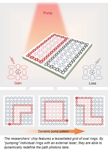
The researchers’ prototype photonic chip is roughly 250 microns squared, and features a tessellated grid of oval rings. By “pumping” the chip with an external laser, targeted to alter the photonic properties of individual rings, they are able to alter which of those rings constitute the boundaries of a waveguide.
The result is a reconfigurable topological insulator. By changing the pumping patterns, photons headed in different directions can be routed around each other, allowing photons from multiple data packets to travel through the chip simultaneously, like a complicated highway interchange.
“We can define the edges such that photons can go from any input port to any output port, or even to multiple outputs at once,” Feng says. “That means the ports-to-footprint ratio is at least two orders of magnitude greater than current state-of-the-art photonic routers and switches.”
Increased efficiency and speed is not the only advantage of the researchers’ approach.
“Our system is also robust against unexpected defects,” Zhao says. “If one of the rings is damaged by a grain of dust, for example, that damage is just making a new set of edges that we can send photons along.”
Since the system requires an off-chip laser source to redefine the shape of the waveguides, the researcher’s system is not yet small enough to be useful for data centers or other commercial applications. Next steps for the team will be to establish a fast reconfiguring scheme in an integrated fashion.
Share on:


Testimonial
"The I-Connect007 team is outstanding—kind, responsive, and a true marketing partner. Their design team created fresh, eye-catching ads, and their editorial support polished our content to let our brand shine. Thank you all! "
Sweeney Ng - CEE PCBSuggested Items
Procense Raises $1.5M in Seed Funding to Accelerate AI-Powered Manufacturing
09/11/2025 | BUSINESS WIREProcense, a San Francisco-based industrial automation startup developing cutting-edge AI and remote sensing technologies for process manufacturers has raised $1.5 million in a seed funding round led by Kevin Mahaffey, Business Insider’s #1 seed investor of 2025 and HighSage Ventures, a Boston-based family office that primarily invests in public and private companies in the global software, internet, consumer, and financial technology sectors.
Zuken Announces E3.series 2026 Release for Accelerated Electrical Design and Enhanced Engineering Productivity
09/10/2025 | ZukenZuken reveals details of the upcoming 2026 release of E3.series, which will introduce powerful new features aimed at streamlining electrical and fluid design, enhancing multi-disciplinary collaboration, and boosting engineering productivity.
AI Infrastructure Boosts Global Semiconductor Revenue Growth to 17.6% in 2025
09/09/2025 | IDCAccording to the Worldwide Semiconduct o r Technology and Supply Chain Intelligence service from International Data Corporation (IDC), worldwide semiconductor revenue is expected to reach $800 billion in 2025, growing 17.6% year-over-year from $680 billion in 2024. This follows a strong rebound in 2024, when revenue grew by 22.4% year-over-year.
I-Connect007 Editor’s Choice: Five Must-Reads for the Week
09/05/2025 | Andy Shaughnessy, I-Connect007It’s almost fall here in Atlanta, and that means that the temperature is finally dropping. And it quit raining! It’s been raining since March, and I’m so over it, as the social influencers say. Last night we grilled out on the deck, and it wasn’t hot, and we didn’t get rained on. Life is good. It was a busy week in the industry. In this installment of my must-reads, we say goodbye to Walt Custer, the man who made PCB data points interesting for the rest of us.
Walt Custer: Making Data Interesting
09/03/2025 | Andy Shaughnessy, I-Connect007I just learned that IPC Hall of Famer Walt Custer has passed away at 81. I first met Walt about 20 years ago when I started covering the fabrication industry. Right away, he started telling me which companies to watch and which trends to follow. This was in the years following 9/11, and things were still pretty fluid.