


 The Right Approach: Get Ready for ISO 9001 Version 6
 Dan’s Biz Bookshelf: ‘Still Broke: Walmart’s Remarkable Transformation'
 Driving Innovation: Depth Routing Processes—Achieving Unparalleled Precision in Complex PCBs


DGIST Achieves the Highest Efficiency of Flexible CZTSSe Thin-Film Solar Cell
September 19, 2019 | DGISTEstimated reading time: 2 minutes
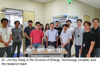
DGIST announced on Tuesday, September 10 that Dr. Jin-Kyu Kang’s research team in Division of Energy Technology achieved 11.4% for the photoelectric conversion efficiency of flexible CZTSSe thin-film solar cell, the highest in the world. This research is expected to contribute to the development of future solar power technology and the thin-film solar cell industry of next generation.
Flexible thin-film solar cell can be applied in various fields such as wearable, building, and automobiles based on the flexible substrate technology. Since CZTSSe thin-film solar cell uses low-cost, ecofriendly materials, it is drawing limelight and is being researched as the next generation solar power technology throughout the world. However, Flexible CZTSSe`s photoelectric conversion efficiency had not exceeded 10% due to technological issue such as the spread of impurities inside the flexible substrate and delamination.
In response, the DGIST research team conducted research and achieved the highest efficiency of 11.4%, which was officially recognized. This achievement is drawing more attention because its mass production is much easier with the use of low-cost, ecofriendly materials such as copper(Cu), zinc(Zn), tin(Sn) than the existing thin-film solar cell (CIGS, CdTe, perovskite2), which uses high-cost heavy metal materials such as indium, lead, and cadmium.
One of the biggest achievements of this research is increased efficiency by changing the existing 3-stack structure of CZTSSe thin-film solar cell precursor into a multi-layered structure and by improving the voltage characteristics and uniformity. Moreover, it has the problem with uniformity degradation when a large-area process is applied to thin-film solar cell, but applied process technology in this research improved not only efficiency but also uniformity.
Dr. Kee-Jeong Yang who led the development of process technology said “Our research achievement has presented ways to secure the uniformity of large-area process, which can cause issues in commercialization. We will be able to advance the commercialization of next generation solar cell which is applicable in various fields such as building outer walls.” Moreover, Senior Researcher Jin-Kyu Kang, the research project manager, said “As there is growing interest towards environment and resources are used unlimitedly these days, it is a very meaningful achievement that we have developed a thin-film solar cell using widely available, ecofriendly materials. We plan to lead the future solar cell technology using widely available materials and contribute to the development of thin-film solar cell industry.
This research was carried out as a project “Development of earth abundant, non-toxic chalcogenide absorber based flexible inorganic thin film solar cell” with support by Korea Energy Technology Evaluation and Planning (KETEP), which is affiliated under the Ministry of Trade, Industry, and Energy. DGIST plans to open the Research Center for Thin Film Solar Cell based on this achievement. Its precursor design technology was published on international journal ‘Nature Communications’ on July 4.
Share on:


Testimonial
"Our marketing partnership with I-Connect007 is already delivering. Just a day after our press release went live, we received a direct inquiry about our updated products!"
Rachael Temple - AlltematedSuggested Items
Closing the Loop on PCB Etching Waste
09/09/2025 | Shawn Stone, IECAs the PCB industry continues its push toward greener, more cost-efficient operations, Sigma Engineering’s Mecer System offers a comprehensive solution to two of the industry’s most persistent pain points: etchant consumption and rinse water waste. Designed as a modular, fully automated platform, the Mecer System regenerates spent copper etchants—both alkaline and acidic—and simultaneously recycles rinse water, transforming a traditionally linear chemical process into a closed-loop system.
Driving Innovation: Depth Routing Processes—Achieving Unparalleled Precision in Complex PCBs
09/08/2025 | Kurt Palmer -- Column: Driving InnovationIn PCB manufacturing, the demand for increasingly complex and miniaturized designs continually pushes the boundaries of traditional fabrication methods, including depth routing. Success in these applications demands not only on robust machinery but also sophisticated control functions. PCB manufacturers rely on advanced machine features and process methodologies to meet their precise depth routing goals. Here, I’ll explore some crucial functions that empower manufacturers to master complex depth routing challenges.
Trouble in Your Tank: Minimizing Small-via Defects for High-reliability PCBs
08/27/2025 | Michael Carano -- Column: Trouble in Your TankTo quote the comedian Stephen Wright, “If at first you don’t succeed, then skydiving is not for you.” That can be the battle cry when you find that only small-diameter vias are exhibiting voids. Why are small holes more prone to voids than larger vias when processed through electroless copper? There are several reasons.
The Government Circuit: Navigating New Trade Headwinds and New Partnerships
08/25/2025 | Chris Mitchell -- Column: The Government CircuitAs global trade winds continue to howl, the electronics manufacturing industry finds itself at a critical juncture. After months of warnings, the U.S. Government has implemented a broad array of tariff increases, with fresh duties hitting copper-based products, semiconductors, and imports from many nations. On the positive side, tentative trade agreements with Europe, China, Japan, and other nations are providing at least some clarity and counterbalance.
How Good Design Enables Sustainable PCBs
08/21/2025 | Gerry Partida, Summit InterconnectSustainability has become a key focus for PCB companies seeking to reduce waste, conserve energy, and optimize resources. While many discussions on sustainability center around materials or energy-efficient processes, PCB design is an often overlooked factor that lies at the heart of manufacturing. Good design practices, especially those based on established IPC standards, play a central role in enabling sustainable PCB production. By ensuring designs are manufacturable and reliable, engineers can significantly reduce the environmental impact of their products.