


 Global PCB Connections: Rigid-flex and Flexible PCBs—The Backbone of Modern Electronics
 Flexible Thinking: The Key to a Successful Flex Circuit Design Transfer
 Happy’s Tech Talk #29: Bend-to-Install Semi-flex FR-4


Research Could Help Flexible Technology Last Longer, Avoid Critical Failures
September 25, 2019 | Binghamton UniversityEstimated reading time: 3 minutes
Whether from regular use, overuse or abuse, every device is bound to develop cracks at some point. That’s just the nature of things.
Cracks can be especially dangerous, though, when working with biomedical devices that can mean life or death to a patient.
A new study from a Binghamton University research team uses the topography of human skin as a model not for preventing cracks but for directing them in the best way possible to avoid critical components and make repairs easy.
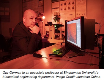
The study, published Sept. 17 in the journal Scientific Reports, is led by Guy German, an associate professor for biomedical engineering in the Thomas J. Watson School of Engineering and Applied Science, and PhD student Christopher Maiorana.
For the study, Maiorana engineered a series of single-layer and dual-layer membranes from silicone-based polydimethylsiloxane (PDMS), an inert and nontoxic material used in biomedical research. Embedded into the layers are tiny channels meant to guide any cracks that form – which, when part of a biomedical device, would give more control over how the cracks form. Potential damage could go around critical areas of flexible electronics, for instance, increasing its functional lifespan.
“In this relatively new field of hyperelastic materials—materials that can really stretch—there’s been a lot of work, but not in the area of fracture control,” German said. “Fracture control has only been explored in more brittle materials.”
What’s particularly important, Maiorana and German said, is having PDMS as the basis for the flexible membrane, since it is known for its wide variety of uses. The study also integrates other common materials.
“We do it without using any exotic material,” Maiorana said. “We’re not inventing some new metal or ceramic. We’re using rubber or modifying normal glass to do these things. We’ve taken this really basic idea and made it functional.”
German’s ongoing research on human skin made him realize that the outermost layer—known as the stratum corneum—exhibits a network of v-shaped topographical microchannels that appear to be capable of guiding fractures to the skin.
This study began with the idea of recreating this effect in nonbiological materials. Previous attempts to direct microcracks have utilized more solid means, such as copper films around the most sensitive parts of flexible electronics components.
“Even though this membrane looks and feels exactly like a normal, boring membrane,” he said, “you stretch it and you can get cracks to deviate at 45-degree angles away from where it ordinarily would have cracked. I think it’s pretty cool.”
Because of the long fabrication period for the membranes, Maiorana often would spend a week to produce one and then tear it apart in a matter of seconds—only to start all over again with the next one. He credited the increasing precision of additive manufacturing and its ability to print ever-smaller features for making the production of the membranes possible.
“Chris was designing his own fabrication systems to make these substrates,” German said, “because he had to 3-D print a mold and then use this clever system to control the depth of these canyons in the substrate. It’s really technically challenging.”
Maiorana added: “There is a certain level of art to it. You think there’s an entire scientific process, and there is, but part of it is that you’ve done this process before and you know what it’s supposed to look like.”
This study, German said, furthers the quest of biomedical engineers to learn from what nature has already perfected. “It doesn’t matter how good an engineer you are—evolution thought of it first,” he said. “Evolution always wins.”
Share on:


Testimonial
"Our marketing partnership with I-Connect007 is already delivering. Just a day after our press release went live, we received a direct inquiry about our updated products!"
Rachael Temple - AlltematedSuggested Items
Closing the Loop on PCB Etching Waste
09/09/2025 | Shawn Stone, IECAs the PCB industry continues its push toward greener, more cost-efficient operations, Sigma Engineering’s Mecer System offers a comprehensive solution to two of the industry’s most persistent pain points: etchant consumption and rinse water waste. Designed as a modular, fully automated platform, the Mecer System regenerates spent copper etchants—both alkaline and acidic—and simultaneously recycles rinse water, transforming a traditionally linear chemical process into a closed-loop system.
Driving Innovation: Depth Routing Processes—Achieving Unparalleled Precision in Complex PCBs
09/08/2025 | Kurt Palmer -- Column: Driving InnovationIn PCB manufacturing, the demand for increasingly complex and miniaturized designs continually pushes the boundaries of traditional fabrication methods, including depth routing. Success in these applications demands not only on robust machinery but also sophisticated control functions. PCB manufacturers rely on advanced machine features and process methodologies to meet their precise depth routing goals. Here, I’ll explore some crucial functions that empower manufacturers to master complex depth routing challenges.
Trouble in Your Tank: Minimizing Small-via Defects for High-reliability PCBs
08/27/2025 | Michael Carano -- Column: Trouble in Your TankTo quote the comedian Stephen Wright, “If at first you don’t succeed, then skydiving is not for you.” That can be the battle cry when you find that only small-diameter vias are exhibiting voids. Why are small holes more prone to voids than larger vias when processed through electroless copper? There are several reasons.
The Government Circuit: Navigating New Trade Headwinds and New Partnerships
08/25/2025 | Chris Mitchell -- Column: The Government CircuitAs global trade winds continue to howl, the electronics manufacturing industry finds itself at a critical juncture. After months of warnings, the U.S. Government has implemented a broad array of tariff increases, with fresh duties hitting copper-based products, semiconductors, and imports from many nations. On the positive side, tentative trade agreements with Europe, China, Japan, and other nations are providing at least some clarity and counterbalance.
How Good Design Enables Sustainable PCBs
08/21/2025 | Gerry Partida, Summit InterconnectSustainability has become a key focus for PCB companies seeking to reduce waste, conserve energy, and optimize resources. While many discussions on sustainability center around materials or energy-efficient processes, PCB design is an often overlooked factor that lies at the heart of manufacturing. Good design practices, especially those based on established IPC standards, play a central role in enabling sustainable PCB production. By ensuring designs are manufacturable and reliable, engineers can significantly reduce the environmental impact of their products.