


 Flexible Thinking: Designing Flex Circuits for Dynamic Reliability
 Global PCB Connections: Rigid-flex and Flexible PCBs—The Backbone of Modern Electronics
 Happy’s Tech Talk #29: Bend-to-Install Semi-flex FR-4


Experts discussed innovative solutions for continued miniaturization, higher power densities, high-speed communication (5G) and electromobility.
At the Red Bull Ring, where high-performance racing cars usually run laps, AT&S presented current trends, challenges and solutions for PCBs and connectivity solutions at the 15th Technology Forum. The choice of venue at the Formula 1 racing circuit highlighted many parallels between the two fields—success in both depends on maximum speed, high efficiency, reliability and innovative cutting-edge technology. Numerous international customers and partners found out about the latest developments in the electronics and PCB industry for areas such as mobile devices, automotive systems, and industrial, communication and medical technology. Expert talks focused on global trends like 5G mobile communications, autonomous driving, electromobility and advancing miniaturization—together with their many challenges.
Spotlight on Technology Trends and Innovations
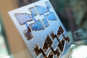
Along with general trends around miniaturization and a status report on current research and development projects, there was a focus on the following key themes: advanced packaging concepts for high-power applications; “cool” solutions for efficient heat dissipation on increasingly complex PCBs; fundamental technologies as a basis for implementing 5G mobile communication; the use of powerful simulation for virtual testing of assembled PCBs and embedded component packages (ECPs); and new technologies for manufacturing large panels (up to 27 inches) and PCBs with more than 50 layers.
“Continuing miniaturization with higher levels of integration and performance on ever smaller board surfaces can only be achieved through higher packing densities of electronic components, which sees PCB and semiconductor technologies converging,” says Walter Moser, CSO of the Automotive, Industrial and Medical business unit at AT&S. “To this end, AT&S offers a combination of established and new technologies that are perfectly matched with each other. One example is a solution using substrate-like PCBs, which permit highly miniaturized and precise structures.”
The roll-out of 5G – the fifth generation of cellular network technology—is a current example of increasing demands on data rates and signal integrity. The same applies to autonomous driving and electromobility. The greatest challenges in implementing 5G hardware, aside from its greater integration density, are reducing signal losses as well as high frequency (HF) and thermal management. AT&S sees the following technologies as key to the implementation of 5G: substrate-like PCBs (mSAP—modified semi-additive process) enable greater functional integration in the Z-axis for smaller overall heights, better signal integrity and better thermal management. Embedding HF components like filters or antennas reduces costs and improves HF characteristics. Embedding technology also brings advantages for further module integration, for example with thermal management components (copper plates, heat pipes, etc.).
With miniaturization and advancing integration, thermal management is becoming increasingly important. Generally, thermal resistance has to be reduced. In turn, this depends on the transfer surface area (the larger the better), conductivity (the higher the better) and the heat transfer path (the shorter the better). At the same time, the interfaces with their thermal contact points should not be overlooked. AT&S addresses the challenges of thermal management with conventional solutions like laser vias or insulated metal substrates (IMS), but also by integrating copper inlays or 2.5D technology with cavities. There are future plans to embed phase-change materials (PCM) close to hot spots or use heat pipes.
AT&S offers some promising solutions for high-power applications to integrate more functions on reduced space. This is especially true for the continuously increasing power density.
Here it is important to evaluate production methods and materials for embedded heterogenous packages to guarantee performance and reliability. Some designs have exhibited problems with copper migration, for example, which could be caused by a variety of factors. AT&S has therefore developed a product-independent leakage testing vehicle (LTV) which avoids time-consuming individual analysis and correlation. It enables corresponding fault analyses, leakage trends and material investigations to be carried out. In addition, powerful simulation tools allow other potential faults (such as warping of the PCB), the inclusion of cavities or the thermal effects of passivation layers to be evaluated in advance.
Building Blocks for All-In-One Packaging
At the close of the Technology Forum, Hannes Voraberger, Director R&D, gave an outlook on R&D activities at AT&S. As of 2019, the company has scaled many innovative technologies into high-volume production. These include embedding passive and power components (embedded component packaging – ECP), using materials with a low dissipation factor (Df), mSAP (30/30 µm), substrate-like PCBs (SLP), and HF processes. Other technologies are in development or already available as prototypes: notable examples are a further reduction in track structures (25 and 20 µm), new thermal concepts, integrated HF solutions, integrated inductors and virtual PCB simulation. On the way to the all-in-one package, AT&S is using various functional modules such as ECP, fan-out system-in-boards (FO-SIBs with power, HF or sensor modules), antenna-in-package (AiP), embedded heat pipes, shielding (metallised cavities), etc.
Investment and Expansion in Substrates
To enable further miniaturization, AT&S in Chongqing has invested in one of the world’s most state-of-the-art production facilities, with a total floor area of 60,000 m². Currently under construction, starting end of 2021 the new plant will produce IC substrates for high-performance computing modules. These provide the basis for the required capabilities of future high-performance applications, enabling the ever-faster processing of constantly growing data volumes – e.g. in artificial intelligence, robotics, autonomous driving and increasingly connected digital systems.
About AT&S
AT&S is the European market leader and one of the globally leading manufacturers of high-value printed circuit boards and IC substrates. AT&S industrialises leading-edge technologies for its core business segments Mobile Devices, Automotive, Industrial, Medical and Advanced Packaging. AT&S has a global presence, with production facilities in Austria (Leoben and Fehring) and plants in India (Nanjangud), China (Shanghai, Chongqing) and Korea (Ansan, near Seoul). The company employed an average of about 10,000 people in the financial year 2017/18. For more information: www.ats.net


