


 It’s Only Common Sense: Hire for Hunger, Train for Skill
 Dan’s Biz Bookshelf: ‘The 'NVIDIA Way: Jensen Huang and the Making of a Tech Giant’


Bigger, Better Conductive Crystals a Boon for Electronics
October 4, 2019 | Agency for Science, Technology and ResearchEstimated reading time: 1 minute
Electronic devices are becoming smaller in size, yet the number of functions each gadget can perform is constantly increasing. Driving these improvements is an essential component known as field-effect transistor (FET). The most common FET in modern times—called MOSFET, short for metal–oxide–semiconductor field-effect transistor—was built using silicon around the end of the 1950s.
However, silicon-based FETs that are miniaturized below a certain size face issues arising from the short channel effect, which negatively impacts the flow and control of electric current. Scientists led by Dongzhi Chi at the Institute of Materials Research and Engineering (IMRE), in collaboration with colleagues at the National University of Singapore and Shenzhen University, China, are now seeking to circumvent this limitation with an alternative material: molybdenum disulfide.
Known to possess high electron mobility and immunity to the short channel effect, molybdenum disulfide is superior to silicon in downscaled digital electronic devices. Yet, growing molybdenum disulfide crystals at scale remains difficult.
“The reported grain size of single-crystal, sulfurization-grown molybdenum disulfide was typically limited to several tens of micrometers or less with conventional molybdenum precursors such as molybdenum metal and molybdenum oxides,” explained IMRE’s Shi Wun Tong, the lead author on the study. “This limited the fabrication and demonstration of high-performance devices on large-area and grain boundary-free molybdenum disulfide single crystals.”
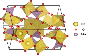
The group therefore explored the use of an alternative crystal precursor, sodium molybdate dihydrate, which not only provides the initial molybdenum for crystal formation, but also enhances the nucleation and lateral growth of the crystal, enabling much larger crystals to be produced. Using this method, the team managed to grow monolayer molybdenum disulfide crystals larger than 300 micrometers.
Remarkably, FETs containing these large monolayer crystals exhibited electron mobility approaching 90 cm2 V-1 s-1, outstripping that of crystals generated through existing methods, which typically display electron mobility ranging between 8–63 cm2 V-1 s-1.
Now, the researchers are looking to incorporate these crystals with various self-powered, ultrathin and flexible electronics. Tong also noted that the ability to synthesize large-sized monolayer crystals paves the way for other applications. “Our approach and findings should enable researchers to design or conduct high-throughput experiments where strictly monolayer and grain boundary-free single crystals are required, such as for quantum optics, valleytronics and piezoelectric applications,” said Tong.
The A*STAR-affiliated researchers contributing to this research are from the Institute of Materials Research and Engineering (IMRE).
Share on:


Testimonial
"We’re proud to call I-Connect007 a trusted partner. Their innovative approach and industry insight made our podcast collaboration a success by connecting us with the right audience and delivering real results."
Julia McCaffrey - NCAB GroupSuggested Items
Long Night of Research 2026: AT&S Brings Artificial Intelligence to Life
04/15/2026 | AT&SWhen the Long Night of Research takes place throughout Austria on Friday, April 24, setting an example for the country’s innovative strength, AT&S will be there with a special highlight.
Foxconn Recognized as Top 100 Global Innovators 2026
04/14/2026 | FoxconnHon Hai Technology Group (Foxconn) has been named in Clarivate’s Top 100 Global Innovators 2026, a milestone for the ninth year running and as the accelerating role of artificial intelligence stood out in innovation activity among peers in the prestigious ranking.
Carbice Awarded Multi-Million Dollar U.S. Navy Contract for Thermal Assembly Joint Technology
04/14/2026 | PRNewswireCarbice, a U.S.-based manufacturer and supplier of novel multifunctional assembly joint technologies, has been awarded a multi-million dollar contract by the U.S. Navy's Office of Naval Research.
Seoul Semiconductor Recognized as a High-Tech Enterprise in Vietnam
04/09/2026 | BUSINESS WIRESeoul Semiconductor Co., Ltd., a leading global opto-semiconductor company, announced that it has officially been granted the “High-Tech Enterprise” certification in Vietnam.
Jon Peddie Research Releases New Photonic AI Processors Report
04/07/2026 | Jon Peddie ResearchJon Peddie Research (JPR), the leading research and consulting firm for graphics and AI technologies, has released its latest report on AI, the Photonic AI Processors report covering developments during the third quarter of 2025.