


 Driving Innovation: Mechanical and Optical Processes During Rigid-flex Production
 It’s Only Common Sense: Your Biggest Competitor Is Complacency
 The Chemical Connection: Onshoring PCB Production—Daunting but Certainly Possible


Spying on Topology
October 4, 2019 | FBHEstimated reading time: 3 minutes
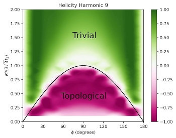
Topological insulators are quantum materials, which, due to their exotic electronic structure, on surfaces and edges conduct electric current like metal, while acting as an insulator in bulk. Scientists from the Max-Born Institute for Nonlinear Optics and Short Pulse Spectroscopy (MBI) have demonstrated for the first time how to tell apart topological materials from their regular—trivial—counterparts within a millionth of a billionth of a second by probing it with ultra-fast laser light. Their method could open the way for such materials to be used as logic elements in light-controlled electronics able to process information tens of thousands times faster as currently possible. Their study appeared in Nature Photonics.
The most common illustration of the topology concept involves an elastic pretzel, which can be stretched, bent, or twisted in any way; no matter the deformation, it is impossible to make a bagel out of a pretzel or add holes to it, without tearing it apart. The number of holes in a pretzel is thus invariant and provides topological information about the pretzel shape.
In a solid material, quantum-mechanical laws restrict which energies electrons can have, leading to the formation of bands with either allowed or forbidden energies. Using the concept of topology, physicists can describe complex shapes of allowed energy bands and assign them a specific topological number. A special topology of the band structure in a material system manifests itself in exotic properties that can be observed—such as the surface conductivity in topological insulators.
“The most remarkable aspect of topology is its robustness: properties induced by topology are protected by it,” explains one of the two main authors of the article Dr. Álvaro Jiménez-Galán from MBI. In the same way that we cannot change the number of holes in a pretzel without breaking it, impurities and other perturbations that usually disrupt the ability of the material to conduct electricity do not affect high electron mobility on the surface of topological insulators. The immunity to impurities is the reason why topological materials strongly appeal to electronic industries.
Making electrons “speak” about topology
Although the topology of the system is deeply linked to the behavior of electrons in it, the imprint of topological properties on electron dynamics at the time scale of a millionth of a billionth of a second has not been discovered up to now. By using numerical simulations and theoretical analysis, the group from MBI has proved that information about system topology is indeed encoded in this extremely fast electron dynamics and can be retrieved by looking at light emitted by electrons as they are excited with laser light. “If we imagine the electrons in a solid moving within energy bands as runners on the racing track, then our method allows to learn about the topology of this racing track, by simply measuring the acceleration of the runners,” clarifies Prof. Dr. Olga Smirnova, head of an MBI Theory group. The ultra-short laser pulses excite electrons of the system, making them hop from one energy band to a higher one, accelerating them on the new track. The accelerated electrons then emit light and quickly fall back to the lower position. This process lasts merely an infinitesimal part of a second but is enough for an electron to “feel” the fine difference between the energy structures of trivial and topological insulators and “encode” this information into the emitted light.
On the way toward ultrafast lightwave electronics
The current work demonstrates how to distinguish between trivial and topological insulators at an ultra-fast rate, in other words, to “read out” the topological information of the system using laser spectroscopy. For the next step, the MBI researchers plan to use this knowledge to convert a trivial insulator into a topological and vice versa with laser light—that is to “write” the topological information into a material at a similar rate. The theoretical proof of this effect could bring forward the implementation of topological materials in optically-controlled electronics, where only the speed of electronic response to light defines the limit for the speed of information processing.
Share on:


Testimonial
"Your magazines are a great platform for people to exchange knowledge. Thank you for the work that you do."
Simon Khesin - Schmoll MaschinenSuggested Items
BAE Contract Agreed with the Republic of Türkiye for Typhoon Aircraft
10/28/2025 | BAE SystemsThe UK Government has announced a c.£5.4 billion agreement with the Republic of Türkiye for the purchase of 20 Typhoon aircraft and an associated weapons and integration package, sustaining more than 20,000 highly skilled jobs across the UK supply chain.
Singapore’s Largest Industrial District Cooling System Begins Operations to Support STMicroelectronics’ Decarbonization Strategy
10/27/2025 | STMicroelectronicsSTMicroelectronics, a global semiconductor leader serving customers across the spectrum of electronics applications, and SP Group (SP), a leading utilities group in the Asia Pacific and Singapore’s national grid operator, have commenced operations for Singapore’s largest industrial district cooling system at STMicroelectronics’ (ST) Ang Mo Kio TechnoPark.
Sensors: The Invisible Force Behind Modern Convenience and Safety
10/24/2025 | Sanjeev Mane, Brooks AutomationSensors and sensor technology are fundamental components of modern life that drive innovation across various electronics and devices. From smartphones to industrial machinery, these small but powerful tools enable seamless interaction with the environment, ensuring efficiency and safety. This article serves as an introduction and overview of sensor technology, highlighting its significance in modern applications and its growing importance in the market as we embrace smarter, more connected systems.
Technica USA Partners with Creative Electron
10/22/2025 | Technica USATechnica USA is proud to announce the partnership with Creative Electron Inc. located in San Marcos, CA.
MES Software Tools Need Thoughtful Integration
10/21/2025 | Nolan Johnson, SMT007 MagazineThe Global Electronics Association recently published a survey report on the state of EMS production software. This project, led by Thiago Guimaraes, director of industry intelligence, connects the dots across the global electronics value chain to uncover practical insights that individual companies might not have seen on their own. In this interview, Thiago discusses the whys and hows of this report.