


 It’s Only Common Sense: Hire for Hunger, Train for Skill
 Dan’s Biz Bookshelf: ‘The 'NVIDIA Way: Jensen Huang and the Making of a Tech Giant’


Advancing World-Class Microelectronics Technology for the Defense Community
October 7, 2019 | BAE SystemsEstimated reading time: 1 minute
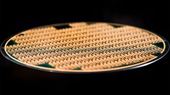
BAE Systems has successfully completed a Phase 1 effort to transition short-gate gallium nitride (GaN) semiconductor technology developed by the U.S. Air Force to our Advanced Microwave Products (AMP) Center. We also were selected by the Air Force Research Laboratory (AFRL) for Phase 2 of the program. The GaN semiconductor technology comes in the form of a wafer that provides high efficiency and broad-frequency bandwidth capabilities in a compact form that can be integrated into a variety of systems to enable next-generation radar, electronic warfare, and communications.
As part of Phase 2, the BAE Systems FAST Labs™ research and development team and the AMP Center will collaborate to further develop and advance the readiness of the technology. Specifically, the project will scale the 140-nanometer GaN monolithic microwave integrated circuit (MMIC) technology to 6-inch wafers and increase its manufacturing level of maturity as part of the validation process, which will include optimizing performance, ensuring process stability, and maximizing wafer-to-wafer uniformity and wafer yields. ENGIN-IC, a custom MMIC design company, will support the design activities, including process design kit validation. This technology will transition to a foundry service product, available through our open foundry service, at the end of Phase 2, where the technology can be leveraged more broadly across different government initiatives.
"Our foundry is a trusted partner to the defense community because it is dedicated to the design, creation, and implementation of vital technologies such as short-gate GaN," said Chris Rappa, product line director for Radio Frequency, Electronic Warfare, and Advanced Electronics at BAE Systems FAST Labs. "GaN technology fills a unique need for the Department of Defense for low-cost, high-performance amplifier technology, and Phase 2 of this effort brings us one step closer to successfully manufacturing and bringing AFRL's technology to market."
BAE Systems is researching and advancing world-class microelectronic technologies, including GaN, in our 70,000-square-foot Microelectronics Center (MEC) located in Nashua, New Hampshire. The MEC has been an accredited DoD Category 1A Trusted Supplier since 2008, and fabricates integrated circuits in production quantities for critical DoD programs.
Share on:


Testimonial
"In a year when every marketing dollar mattered, I chose to keep I-Connect007 in our 2025 plan. Their commitment to high-quality, insightful content aligns with Koh Young’s values and helps readers navigate a changing industry. "
Brent Fischthal - Koh YoungSuggested Items
Long Night of Research 2026: AT&S Brings Artificial Intelligence to Life
04/15/2026 | AT&SWhen the Long Night of Research takes place throughout Austria on Friday, April 24, setting an example for the country’s innovative strength, AT&S will be there with a special highlight.
Foxconn Recognized as Top 100 Global Innovators 2026
04/14/2026 | FoxconnHon Hai Technology Group (Foxconn) has been named in Clarivate’s Top 100 Global Innovators 2026, a milestone for the ninth year running and as the accelerating role of artificial intelligence stood out in innovation activity among peers in the prestigious ranking.
RTX's Raytheon Unveils First Event-Based MWIR Camera for Real-Time High-Speed Threat Tracking
04/13/2026 | PRNewswireRaytheon, an RTX business, successfully demonstrated a new event-based mid-wave infrared (MWIR) camera that tracks high speed objects in real time while dramatically reducing processing and power demands.
SMTA Ultra HDI Symposium, Day 1: AI at the Core or Out of the Game
04/13/2026 | Marcy LaRont, I-Connect007It was a beautiful 81°F morning in Arizona last Wednesday as I headed to the third annual SMTA Ultra HDI Symposium, focused on AI and ultra high density interconnect technology. Strategically held as part of Arizona’s Tech Week, this year’s conference took place in Avondale in Phoenix's West Valley. The event moved from the cozy offices of the Peoria Sports Complex (which paid homage to baseball’s spring training world) to the larger Avondale Conference Center, highlighting the importance of this area for electronics manufacturing investment.
Gartner Forecasts Worldwide Semiconductor Revenue to Exceed $1.3 Trillion in 2026
04/10/2026 | Gartner, Inc.Global semiconductor revenue is projected to exceed $1.3 trillion in 2026, exhibiting the highest growth in the last two decades, according to Gartner, Inc., a business and technology insights company.