


 Happy’s Tech Talk #40: Factors in PTH Reliability—Hole Voids
 Facing the Future: Time for Real Talk, Early and Often, Between Design and Fabrication
 Trouble in Your Tank: Can You Drill the Perfect Hole?


New High-speed 3D Surface Imaging Technology in Electronics Manufacturing Applications
October 9, 2019 | Juha Saily, Focalspec Inc.Estimated reading time: 2 minutes
Introduction
Line confocal sensors—and scanners based on them—are used in the imaging of surfaces, transparent materials, and multi-layered structures in various metrology and inspection applications on discrete parts, assemblies, webs, and other continuous products. Examples of well-suited applications for line confocal technology include glossy, mirror-like, transparent and multi-layered surfaces made of metals (connector pins, conductor traces, solder bumps, etc.), polymers (adhesives, enclosures, coatings, etc.), ceramics (components, substrates, etc.) and glass (display panels, etc.). Line confocal sensors operate at high speed and can be used to scan fast-moving surfaces in real-time as well as stationary product samples in the laboratory.
Imaging results can be used to characterize a product’s dimensions, form, surface topography, surface roughness, flatness, thickness, and 3D volume. The line confocal method also has a tomographic functionality, which enables the capture of 3D structures under transparent layers, as well as the simultaneous acquisition of 2D gray-scale (intensity) images from single or multiple surfaces with a large depth of focus covering the sensor’s entire Z range (up to 5.50 mm).
Line Confocal Method
Figure 1 shows the line confocal sensor models that are currently in production. Each sensor has two front lenses—one for its transmitter and another for the receiver.
Figure 2: Line confocal method principle.
Figure 2 depicts the sensor’s operating principle. The transmitter has a light source that emits white light containing all visible wavelengths. An optical assembly separates the light into wavelengths and focuses each color at a different distance from the sensor, forming a focal plane.
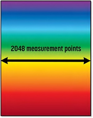
Depending on the vertical position of the imaged surface within the plane, corresponding wavelengths from 2,048 lateral points are reflected back to the sensor’s receiver. The receiver’s spectral camera captures wavelength and intensity information from each point to form related height and gray-scale profile lines. When the surface is moved in front of the sensor, a 3D point cloud and 2D grayscale image are generated from the scanned area line by line. The resulting data can be processed, analyzed, and reported with various 3D surface analysis and image processing software packages.
Line Confocal Method Imaging Capabilities
The line confocal sensors and systems work well in applications that require high-speed imaging of challenging materials at sub-micron resolution. Scanning an area that would require minutes or hours for traditional 3D imaging methods, such as point confocal or interferometric technologies, can be completed within a few seconds.
Transparent materials and products with highly reflective or mirror-like surfaces are ideal for the line confocal method. The sensors’ large numerical aperture and high tolerance for surface angle allow for imaging of steep slopes and glossy curved surfaces. This method does not suffer from speckle noise; this enables surface imaging at a much higher resolution than laser triangulation sensors.
The quality of the raw image data produced by the line confocal sensors is good and rarely needs filtering or other manipulation of any kind. Since the sensors capture 2,048 measurement points simultaneously, the vibration of the imaged surface or the sensor itself seldom causes issues; relative point height positions within the measurement profile line remain unaffected.
To read the full article, which appeared in the September 2019 issue of PCB007 Magazine, click here.
Share on:


Suggested Items
KYZEN to Highlight Understencil and PCB Cleaners at SMTA Querétaro Expo and Tech Forum
07/09/2025 | KYZEN'KYZEN, the global leader in innovative environmentally responsible cleaning chemistries, will exhibit at the SMTA Querétaro Expo & Tech Forum, scheduled to take place Thursday, July 24, at Centro de Congresos y Teatro Metropolitano de Querétaro.
Driving Innovation: Direct Imaging vs. Conventional Exposure
07/01/2025 | Simon Khesin -- Column: Driving InnovationMy first camera used Kodak film. I even experimented with developing photos in the bathroom, though I usually dropped the film off at a Kodak center and received the prints two weeks later, only to discover that some images were out of focus or poorly framed. Today, every smartphone contains a high-quality camera capable of producing stunning images instantly.
Hands-On Demos Now Available for Apollo Seiko’s EF and AF Selective Soldering Lines
06/30/2025 | Apollo SeikoApollo Seiko, a leading innovator in soldering technology, is excited to spotlight its expanded lineup of EF and AF Series Selective Soldering Systems, now available for live demonstrations in its newly dedicated demo room.
Indium Corporation Expert to Present on Automotive and Industrial Solder Bonding Solutions at Global Electronics Association Workshop
06/26/2025 | IndiumIndium Corporation Principal Engineer, Advanced Materials, Andy Mackie, Ph.D., MSc, will deliver a technical presentation on innovative solder bonding solutions for automotive and industrial applications at the Global Electronics A
Fresh PCB Concepts: Assembly Challenges with Micro Components and Standard Solder Mask Practices
06/26/2025 | Team NCAB -- Column: Fresh PCB ConceptsMicro components have redefined what is possible in PCB design. With package sizes like 01005 and 0201 becoming more common in high-density layouts, designers are now expected to pack more performance into smaller spaces than ever before. While these advancements support miniaturization and functionality, they introduce new assembly challenges, particularly with traditional solder mask and legend application processes.