


 It’s Only Common Sense: Stay Curious, My Friends
 The Marketing Minute: AI Is Watching Your Marketing Habits


Researchers at EPFL have created a metallic microdevice in which they can define and tune patterns of superconductivity. Their discovery, which holds great promise for quantum technologies of the future, has just been published in Science.
Superconductivity has fascinated scientists for many years since it offers the potential to revolutionize current technologies. Materials only become superconductors—meaning that electrons can travel in them with no resistance—at very low temperatures. These days, this unique zero resistance superconductivity is commonly found in a number of technologies, such as magnetic resonance imaging (MRI). Future technologies, however, will harness the total synchrony of electronic behavior in superconductors—a property called the phase. There is currently a race to build the world’s first quantum computer, which will use these phases to perform calculations. Conventional superconductors are very robust and hard to influence, and the challenge is to find new materials in which the superconducting state can be easily manipulated in a device.
EPFL’s Laboratory of Quantum Materials (QMAT), headed by Philip Moll, professor at the School of Engineering, has been working on a specific group of unconventional superconductors known as heavy fermion materials. The QMAT scientists, as part of a broad international collaboration between EPFL, the Max Planck Institute for Chemical Physics of Solids, the Los Alamos National Laboratory and Cornell University, made a surprising discovery about one of these materials, CeIrIn5.
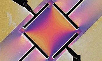
CeIrIn5 is a metal that superconducts at a very low temperature, only 0.4°C above absolute zero (around -273°C). The QMAT scientists, together with Katja C. Nowack from Cornell University, have now shown that this material could be produced with superconducting regions coexisting alongside regions in a normal metallic state. Better still, they produced a model that allows researchers to design complex conducting patterns and, by varying the temperature, to distribute them within the material in a highly controlled way. Their research has just been published in Science.
To achieve this feat, the scientists sliced very thin layers of CeIrIn5—only around a thousandth of a millimeter thick—that they joined to a sapphire substrate. When cooled, the material contracts significantly whereas the sapphire contracts very little. The resulting interaction puts stress on the material, as if it were being pulled in all directions, thus slightly distorting the atomic bonds in the slice. As the superconductivity in CeIrIn5 is unusually sensitive to the material’s exact atomic configuration, engineering a distortion pattern is all it takes to achieve a complex pattern of superconductivity. This new approach allows researchers to “draw” superconducting circuitry on a single crystal bar, a step that paves the way for new quantum technologies.
The image illustrates the temperature evolution of the spatially modulated superconducting state
This discovery represents a major step forward in controlling superconductivity in heavy fermion materials. But that’s not the end of the story. Following on from this project, a post-doc researcher has just begun exploring possible technological applications.
“We could, for example, change the regions of superconductivity by modifying the material’s distortion using a microactuator,” says Moll. “The ability to isolate and connect superconducting regions on a chip could also create a kind of switch for future quantum technologies, a little like the transistors used in today’s computing.”


