


 It’s Only Common Sense: Hire for Hunger, Train for Skill
 Dan’s Biz Bookshelf: ‘The 'NVIDIA Way: Jensen Huang and the Making of a Tech Giant’


Living on the Edge: How a 2D Material Got Its Shape
October 25, 2019 | Lawrence Berkeley National LaboratoryEstimated reading time: 4 minutes
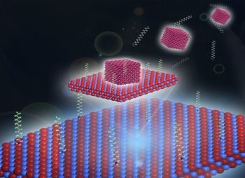
Ever since its discovery in 2004, graphene—an atomically thin material with amazing strength and electrical properties—has inspired scientists around the world to design new 2D materials to serve a broad range of applications, from renewable energy and catalysts to microelectronics.
While 2D structures form naturally in materials like graphene, some scientists have sought to make 2D materials from semiconductors called transition metal oxides: compounds composed of oxygen atoms bound to a transition metal such as cobalt. But while scientists have long known how to make nanoparticles of transition metal oxides, no one has found a controllable way to grow these 3D nanoparticles into nanosheets, which are thin 2D materials just a few atoms thick.
Now, a team of scientists led by the Department of Energy’s Lawrence Berkeley National Laboratory (Berkeley Lab) has gained valuable insight into 3D transition metal oxide nanoparticles’ natural “edge” for 2D growth. Their findings were reported in Nature Materials.
Using a liquid-phase transmission electron microscope (TEM) at Berkeley Lab’s Molecular Foundry for the experiments, co-corresponding author Haimei Zheng and her team directly observed the dynamic growth of cobalt-oxide nanoparticles in a solution, and their subsequent transformation into a flat 2D nanosheet.
“Such a 3D to 2D transformation is much like the white of an egg spreading as it fries in a pan,” said Zheng, a senior staff scientist in Berkeley Lab’s Materials Sciences Division who led the study.
In previous studies, scientists had assumed that only two major factors—bulk energy from the volume of the nanoparticles, and the nanoparticles’ surface energy—would drive the nanoparticles’ growth into a 3D shape, Zheng explained.
New Energy Comes to Light
But calculations led by co-corresponding author Lin-Wang Wang revealed another energy that had been previously overlooked—edge energy. In a faceted, rectangular nanoparticle such as a transition metal oxide nanoparticle, the edge of a facet also contributes energy—in this case, positive energy—toward the nanoparticle’s growth and shape. But in order for a transition metal oxide nanoparticle to grow into a 2D nanosheet, the surface energy must be negative.
“And it’s the balance between these two energies, one negative and one positive, which determines the shape change,” Wang said. For smaller nanoparticles, positive edge energy wins, which leads to a compact 3D shape. But when the cobalt oxide nanoparticles grow larger, they ultimately reach a critical point where negative surface energy wins, resulting in a 2D nanosheet, he explained. Wang, a senior staff scientist in Berkeley Lab’s Materials Sciences Division, performed the calculations for the study on supercomputers at Berkeley Lab’s National Energy Research Scientific Computing Center (NERSC).
Uncovering these growth pathways, including the 3D-to-2D transition, Zheng added, provides new opportunities for the streamlined design of exotic new materials from compounds whose irregular atomic structures, such as transition metal oxides, are more challenging than graphene to synthesize into multilayered 2D devices.
Schematic illustrating the growth of 3D nanoparticles from a solution, and the 3D nanoparticles transformation into 2D nanosheets. (Credit: Haimei Zheng/Berkeley Lab)
Zheng and her team concluded that the study could not have been possible with a conventional electron microscope. By using liquid-phase TEM at the Molecular Foundry, the researchers were able to study the growth of atomically thin materials in solution by encapsulating the liquid sample in a specially designed liquid cell. The cell prevented the sample from collapsing in the high vacuum of the electron microscope.
“It would be impossible to know such a growth path without this in situ observation,” said first author Juan Yang, who was a visiting doctoral researcher at Berkeley Lab from Dalian University of Technology of China at the time of the study. “This discovery may transform our future design of materials with surface-enhanced properties for catalysis and sensing applications of the future.”
Next Steps
The researchers' next plan to focus on using liquid-cell TEM to grow more complex 2D materials such as heterostructures, which are like sandwiches of layered materials with different properties.
“Like an architect who is inspired by the way in which an ancient giant redwood has grown, materials scientists are inspired to design ever more complex structures for energy storage,” said Zheng, who pioneered liquid-cell TEM at Berkeley Lab in 2009. “But why do they grow that way? Our strength at Berkeley Lab is that we can study them at the atomic level and watch them grow in real time and figure out the mechanisms that would contribute to the design of better materials.”
This work was supported by the DOE Office of Science’s Basic Energy Sciences program and included research at the Molecular Foundry and National Energy Research Scientific Computing Center, which are DOE Office of Science User Facilities.
Video: Cobalt-oxide nanoparticles in a solution transform into flat 2D nanosheets; video plays 15 times faster than real time. 3D to 2D growth observed using liquid-phase transmission electron microscopy at Berkeley Lab’s Molecular Foundry. (Credit: Haimei Zheng/Berkeley Lab)
Share on:


Testimonial
"The I-Connect007 team is outstanding—kind, responsive, and a true marketing partner. Their design team created fresh, eye-catching ads, and their editorial support polished our content to let our brand shine. Thank you all! "
Sweeney Ng - CEE PCBSuggested Items
AGC's Advanced PCB Material Solutions
04/17/2026 | Real Time with... APEX EXPOAGC's line includes advanced PCB materials for critical industries such as aerospace, defense, and medical. This interview highlights their commitment to North American sourcing, offering solutions to today's challenges. AGC provides specialized automotive PCB materials including fastRise, a low-loss non-reinforced prepreg designed for high-frequency applications like 77 GHz radar.
What’s Next for PCB Materials? I-Connect007 Podcast Series Turns to Supply Chain Resilience
04/16/2026 | I-Connect007 Editorial TeamI-Connect007 continues its six-part podcast series with Isola experts titled, PCB Materials: The Backbone and Future of Electronics, with the release of Episode 5, which shifts focus to one of the industry’s most urgent challenges: supply chain resilience.
Indium Showcases Solder Alloy Reliability Research for Heterogeneous Integration at ICEP-HBS
04/15/2026 | Indium CorporationIndium Corporation Senior Global Product Manager, Semiconductor and Advanced Materials, Sze Pei Lim will present a collaborative International Electronics Manufacturing Initiative (INEMI) project comparing SnBi and SAC305 solder alloys for first-level interconnects in complex heterogeneous packages.
Podcast Hits the Mark in a Materials Market
04/15/2026 | Marcy LaRont, I-Connect007The base material of a printed circuit board is its literal and functional foundation. Isola, founded in 1912 in Düren, Germany, is one of the longest-standing manufacturers of glass-reinforced laminates in the electronics industry. Originally focused on insulation and fiberglass materials, the company played an early role in supplying the foundational substrates that enabled the growth of PCB technology. As electronics advanced, Isola evolved alongside the industry, expanding from basic glass-epoxy laminates into high-performance copper-clad materials and engineered prepregs.
SMTA Ultra HDI Symposium, Day 2: Fragile Supply Chains, Fierce Innovation
04/14/2026 | Marcy LaRont, I-Connect007The Arizona weather yielded another beautiful day as we gathered for the second day of SMTA’s annual UHDI symposium. After the first full day discussing the role of AI in business and the how-tos of implementation, Avondale Mayor Mike Pineda kicked off day two, proud to showcase his city and to declare its important place in the continued development of the West Valley, an increasingly important area for tech and manufacturing.