


 The Hidden Enabler of Autonomous Warfare: Advanced PCB Technologies Behind Defense AI
 It’s Only Common Sense: Stay Curious, My Friends


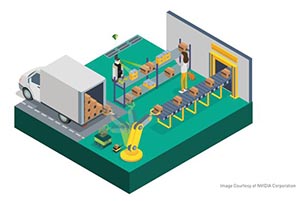
NVIDIA has announced that the United States Postal Service—the world’s largest postal service, with 485 million mail pieces processed and delivered daily—is adopting end-to-end AI technology from NVIDIA to improve its package data processing efficiency.
The new system starts with high-performance servers powered by NVIDIA V100 Tensor Core GPUs and deep learning software to train multiple AI algorithms. The trained models are then deployed to NVIDIA EGX edge computing systems at close to 200 Postal Service facilities throughout the U.S. to enable more efficient package data processing. The NVIDIA-powered systems are being purchased by the Postal Service under contract with Hewlett Packard Enterprise.
“AI is transforming multiple industries, enabling processes, accuracy and efficiency not possible before,” said Anthony Robbins, vice president of the Federal Sector Business at NVIDIA. “The U.S. Postal Service’s adoption of AI demonstrates how this powerful technology can improve an excellent service that we rely on every day. Benjamin Franklin would be proud.”
The Postal Service operates the world’s highest volume logistics operation, processing and delivering some 146 billion pieces of mail annually, including more than 6 billion packages. The new AI system will process package data 10x faster and with higher accuracy.
Engineering teams from the Postal Service and NVIDIA have been collaborating for several months to develop AI models, using NVIDIA software including TensorRT™ for high-throughput, low-latency inference optimization; automatic mixed precision in PyTorch to accelerate training while maintaining model accuracy; NGC containers, which are GPU-optimized for streamlining software deployment; and DeepOps tools for optimizing GPU clusters.
Delivery and testing of the system will start this year and it is expected to be fully operational by spring of 2020.


