


 Global PCB Connections: Rigid-flex and Flexible PCBs—The Backbone of Modern Electronics
 Flexible Thinking: The Key to a Successful Flex Circuit Design Transfer
 Happy’s Tech Talk #29: Bend-to-Install Semi-flex FR-4


Machine Vision Products Introduces Versa AOI/SPI Solution
February 3, 2020 | Machine Vision ProductsEstimated reading time: 1 minute
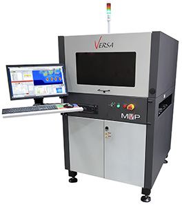
Building on MVP’s 25 years’ experience of innovative Automated Optical Inspection the Versa system brings the latest 3D technologies to MVPs SMT and SPI offerings and is a significant advance in the flexibility of PCB assembly inspection.
Uniquely, MVP’s Versa system allows fast programming and the flexibility to fit into all the processes in the line: Paste Inspection, Pre-Reflow, Post-Reflow, Post-Wave and Selective Solder.
The Versa system, is the first introduction in a new series of MVP 3D AOI products distinguished by: high-performance defect detection, lowest over-rejection and a low cost of ownership. With the enhanced 3D capabilities, the Versa maintains MVP’s flagship process flexibility and scalability.
Cultivating on our expertise in defect detection for SMT and microelectronics inspection, MVP’s Versa allows for versatile program strategies in a single software toolset.
Using MVP’s ease-of-use ePro software guides you through the program generation process allowing for each inspection strategy to be developed quickly and automatically.
Import capabilities include Gerber, ODB++ and a variety of other formats. Combined with MVP’s leading-edge optimization tools for high performance and minimized over rejection, ease-of-use and rapid programming has been a paramount objective for our latest software suite.
Designed with future technology trends in mind, Versa’s 3D and optical capabilities provide high accuracy measurement capabilities for all current and future paste and SMT inspection. The Versa has multiple 3D options for even the most complex of inspection challenges
Using standard software and hardware across the Versa’s cross-process capability allows you to reduced support costs as you only need to provide support and training for a single platform vs. multiple different system. MVP’s leading reliability allows you to obtain the highest performance and uptime from your investments.
Visit MVP at IPC Apex 2020 at booth 1800 to see and have a demonstration of our latest SMT and Microelectronics Inspection Solutions.
Share on:


Testimonial
"Our marketing partnership with I-Connect007 is already delivering. Just a day after our press release went live, we received a direct inquiry about our updated products!"
Rachael Temple - AlltematedSuggested Items
Koh Young, Fuji, and Kurtz ERSA Drive Smart Manufacturing Solutions for EV and Automotive Electronics at Kunshan, China Technical Seminar
09/11/2025 | Koh YoungKoh Young Technology, the global leader in True 3D measurement-based inspection solutions, partnered with Fuji Corporation and Kurtz ERSA to host an exclusive technical seminar for leading automotive manufacturers in East China. Held on September 4 at Fuji’s factory in Kunshan, the event gathered participants representing over 35 companies.
MacDermid Alpha Presents at SMTA New Delhi, Bangalore Chapter, on Flux–OSP Interaction
09/09/2025 | MacDermid Alpha Electronics SolutionsMacDermid Alpha contributes technical insights on OSP solderability at the Bangalore Chapter, SMTA reinforcing commitment to knowledge-sharing and industry collaboration.
Electra’s ElectraJet EMJ110 Inkjet Soldermask Now in Black & Blue at Sunrise Electronics
09/08/2025 | Electra Polymers LtdFollowing the successful deployment of Electra’s Green EMJ110 Inkjet Soldermask on KLA’s Orbotech Neos™ platform at Sunrise Electronics in Elk Grove Village, Illinois, production has now moved beyond green.
Absolute EMS: The Science of the Perfect Solder Joint
09/05/2025 | Absolute EMS, Inc.Absolute EMS, Inc., a six-time award-winning provider of fast turnaround, turnkey contract electronic manufacturing services (EMS), is drawing attention to the critical role of 3D Solder Paste Inspection (SPI) in ensuring the reliability of both FLEX and rigid printed circuit board assemblies (PCBAs).
Indium Corporation to Highlight High-Reliability Solder Solutions at SMTA Guadalajara Expo
09/04/2025 | Indium CorporationIndium Corporation, a leading materials refiner, smelter, manufacturer, and supplier to the global electronics, semiconductor, thin-film, and thermal management markets, will feature a range of innovative, high-reliability solder products for printed circuit board assembly (PCBA) at the SMTA Guadalajara Expo and Tech Forum, to be held September 17-18 in Guadalajara, Mexico.