StratEdge Features Semiconductor Packages and Assembly Services at Three Trade Shows in March
February 25, 2020 | StratEdgeEstimated reading time: 1 minute

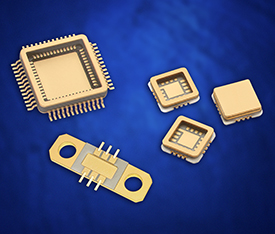
StratEdge Corporation, leader in the design, production, and assembly of high-frequency and high-power semiconductor packages for microwave, millimeter-wave, and high-speed digital devices, will have applications specialists available at the IMAPS Device Packaging Conference, APEC 2020, and GOMACTech 2020 to discuss the many packages available for DC to 63+ GHz and its package assembly services.
Packages include:
- Post-fired ceramic, low-cost molded ceramic, and ceramic QFN packages
- The LL family of leaded laminate copper-moly-copper (CMC) base packages
- High-power semiconductor packages
- Off-the-shelf molded ceramic packages that can be configured to meet the requirements for chips with frequencies up to 18 GHz. These packages provide enhanced thermal dissipation for high-power gallium nitride devices and come in fully hermetic versions in over 200 standard outlines.
- High-reliability packages that meet stringent military applications. The packages have electrical transition designs that ensure exceptionally low electrical losses and operate efficiently, even at the highest frequencies.
"Much attention is given to GaN chips, but the package in which the GaN device is attached and the way the chip is attached to the package is often overlooked," explained Casey Krawiec, VP of global sales for StratEdge Corporation. "It's well known that GaN chip efficiency and reliability can be improved by creating a package environment that reduces chip-to-package junction temperatures. StratEdge has developed a proprietary eutectic die attach method that drops junction temperatures by 20 degrees when compared to standard assembly methods with ceramic packages. Please stop by our booths and find out more."
StratEdge will be at IMAPS Device Packaging Conference, Fountain Hills, AZ, from March 3-4 in booth 56, APEC 2020, New Orleans, LA, from March 16-18 in booth 2157, and at GOMACTech 2020, San Diego, CA, from March 17-18, in booth 202.
Testimonial
"Advertising in PCB007 Magazine has been a great way to showcase our bare board testers to the right audience. The I-Connect007 team makes the process smooth and professional. We’re proud to be featured in such a trusted publication."
Klaus Koziol - atgSuggested Items
Closing the Loop on PCB Etching Waste
09/09/2025 | Shawn Stone, IECAs the PCB industry continues its push toward greener, more cost-efficient operations, Sigma Engineering’s Mecer System offers a comprehensive solution to two of the industry’s most persistent pain points: etchant consumption and rinse water waste. Designed as a modular, fully automated platform, the Mecer System regenerates spent copper etchants—both alkaline and acidic—and simultaneously recycles rinse water, transforming a traditionally linear chemical process into a closed-loop system.
Driving Innovation: Depth Routing Processes—Achieving Unparalleled Precision in Complex PCBs
09/08/2025 | Kurt Palmer -- Column: Driving InnovationIn PCB manufacturing, the demand for increasingly complex and miniaturized designs continually pushes the boundaries of traditional fabrication methods, including depth routing. Success in these applications demands not only on robust machinery but also sophisticated control functions. PCB manufacturers rely on advanced machine features and process methodologies to meet their precise depth routing goals. Here, I’ll explore some crucial functions that empower manufacturers to master complex depth routing challenges.
Trouble in Your Tank: Minimizing Small-via Defects for High-reliability PCBs
08/27/2025 | Michael Carano -- Column: Trouble in Your TankTo quote the comedian Stephen Wright, “If at first you don’t succeed, then skydiving is not for you.” That can be the battle cry when you find that only small-diameter vias are exhibiting voids. Why are small holes more prone to voids than larger vias when processed through electroless copper? There are several reasons.
The Government Circuit: Navigating New Trade Headwinds and New Partnerships
08/25/2025 | Chris Mitchell -- Column: The Government CircuitAs global trade winds continue to howl, the electronics manufacturing industry finds itself at a critical juncture. After months of warnings, the U.S. Government has implemented a broad array of tariff increases, with fresh duties hitting copper-based products, semiconductors, and imports from many nations. On the positive side, tentative trade agreements with Europe, China, Japan, and other nations are providing at least some clarity and counterbalance.
How Good Design Enables Sustainable PCBs
08/21/2025 | Gerry Partida, Summit InterconnectSustainability has become a key focus for PCB companies seeking to reduce waste, conserve energy, and optimize resources. While many discussions on sustainability center around materials or energy-efficient processes, PCB design is an often overlooked factor that lies at the heart of manufacturing. Good design practices, especially those based on established IPC standards, play a central role in enabling sustainable PCB production. By ensuring designs are manufacturable and reliable, engineers can significantly reduce the environmental impact of their products.