


 The Hidden Enabler of Autonomous Warfare: Advanced PCB Technologies Behind Defense AI
 It’s Only Common Sense: Stay Curious, My Friends


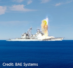
BAE Systems Inc. was awarded a five-year $188.2 million contract to provide the U.S. Navy’s AEGIS Technical Representative (AEGIS TECHREP) organization with critical large-scale system engineering, integration, and testing expertise for the AEGIS Weapons and Combat Systems aboard U.S. Navy surface combatant ships.
“BAE Systems personnel have worked side-by-side with Navy sailors and civilians for nearly 40 years to strengthen and modernize the fleet of AEGIS-equipped surface ships,” said Mark Keeler, vice president and general manager of BAE Systems’ Integrated Defense Solutions business. “Our team brings a wealth of AEGIS combat system expertise with the agility, innovation, and technical acumen to ensure the U.S. Navy has the safe and effective combat capability it needs to meet mission objectives.”
As part of the AEGIS Technical Representative Engineering Support Services contract, BAE Systems will provide Navy acquisition managers with on-site leadership and systems engineering to validate Total Ship Combat design at Navy sites in Mt. Laurel, New Jersey; Bath, Maine; and Pascagoula, Mississippi. The company also will support systems engineering and test and evaluation personnel to provide fleet experience and operational insight. Additionally, the company will provide logistics, cybersecurity, production, acquisition, and waterfront support required for upgrading and maintaining development of AEGIS Combat System capabilities and baselines across the entire life cycle.
BAE Systems delivers a broad range of services and solutions enabling militaries and governments to successfully carry out their respective missions. The company provides large-scale systems engineering, integration, and sustainment services across air, land, sea, space, and cyber domains. BAE Systems takes pride in its support of national security and those who serve.


