


 Flexible Thinking: Designing Flex Circuits for Dynamic Reliability
 Global PCB Connections: Rigid-flex and Flexible PCBs—The Backbone of Modern Electronics
 Happy’s Tech Talk #29: Bend-to-Install Semi-flex FR-4


New Optical System Could Lead to Devices That Can Recognize Objects Instantly
March 9, 2020 | UCLA NewsroomEstimated reading time: 2 minutes
A technology developed at the UCLA Samueli School of Engineering could one day make it possible to produce optical devices that can instantaneously recognize objects without additional computer processing. The technology could ultimately be useful for robots, autonomous vehicles and other applications.
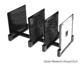
The UCLA researchers developed an optical neural network, a “maze” for beams of light, with a series of specially designed translucent wafers made of different materials such as plastic or glass. The wafers have rough surfaces — similar to frosted glass — which are designed at a scale smaller than the wavelength of light to split up light beams into various directions as they travel through the maze.
The research is described in a study published in Light: Science & Applications.
Because of how the light interacts with the wafers, each sub-band of light exiting the maze is precisely directed to a desired spot on a screen at the end of the array. That’s possible because the device can simultaneously process many wavelengths of light, in contrast to previous similar devices, also created by UCLA engineers, that could only use a single wavelength. Those earlier devices were able to identify handwritten numbers and clothing items, which are commonly used in tests of artificial intelligence systems.
“The advance is like the transition from black-and-white TV to color TV,” said Aydogan Ozcan, who led the study and is a UCLA chancellor’s professor of electrical and computer engineering. “There is richer information when you can see colors through different wavelengths of light. Most scenes naturally contain information in vivid color, so the more wavelengths that a network can ‘see,’ the more it increases the amount of information it can process.”
The beam of light that the engineers directed into the maze was composed of many wavelengths in the terahertz part of the light spectrum.
“One of the goals of this research is to create a technology that intuitively combines the capabilities of our eyes and brains, and this new study is a step toward that,” said Ozcan, who also is the associate director of the California NanoSystems Institute at UCLA. “Ultimately, we want to expand the technical capabilities of optical computation and design beyond that of human capabilities.”
The network was designed using a branch of artificial intelligence called deep learning, in which computer programs “learn” and adjust their responses accordingly based on numerous repetitions of an action or experiment.
“Traditionally, researchers use their own knowledge of physics and intuition to design optical mazes that harness and engineer light in unique ways,” Ozcan said. “Now, deep learning is surprising us in finding new methods — ones that we would normally not come up with — to solve these puzzles. It’s helping us design new optical devices that provide powerful and elegant solutions to challenging problems.”
The study’s other authors are graduate students Yi Luo, Deniz Mengu and Muhammed Veli; postdoctoral researcher Nezih Yardimci; adjunct professor Yair Rivenson; and professor Mona Jarrahi — all of whom are members of UCLA’s electrical and computer engineering department.
The study was supported in part by Fujikura, a Japanese electronics equipment manufacturer. News from Matthew Chin.
Share on:


Testimonial
"In a year when every marketing dollar mattered, I chose to keep I-Connect007 in our 2025 plan. Their commitment to high-quality, insightful content aligns with Koh Young’s values and helps readers navigate a changing industry. "
Brent Fischthal - Koh YoungSuggested Items
Bell Selected by Near Earth Autonomy to Supply Bell 505 for U.S. Marine Corps MARV-EL Program
05/01/2026 | BellBell Textron Inc., a Textron Inc. company, announced that it was selected by Near Earth Autonomy (Near Earth) as a partner on the prototyping of an autonomous Bell 505 for the U.S. Marine Corps’ Aerial Resupply Vehicle - Expeditionary Logistics (MARV-EL) Increment 2 program.
Boeing, U.S. Navy Achieve Successful MQ-25A Test Flight
04/28/2026 | BoeingBoeing and the U.S. Navy have successfully completed the first test flight of an operational MQ-25A Stingray™.
Bellatrix Lands $20M Pre-Series B for Global Expansion
04/02/2026 | BellatrixBellatrix Aerospace, a leading In-Space Mobility company from India with a presence in the USA, announced that it has closed a US$20 million Pre-Series B growth round led by Cactus Partners, marking a significant milestone as the company accelerates the commercialization and delivery of its propulsion systems.
Akrometrix Discusses AI Chip Board Demands
03/27/2026 | Real Time with... APEX EXPOPaul Handler of Akrometrix discusses the evolving demands in PCB fabrication, particularly the surge in large-format, room-temperature boards for AI chips. He highlights the critical need for inline, real-time testing of heavy, high-value circuit boards and Akrometrix's strategic shift towards integrated Industry 4.0 solutions. Handler also highlights the engineering challenges and the company's positive outlook for industry growth.
DARPA-developed Autonomous Helicopter Technology Transitions to U.S. Army
03/23/2026 | DARPADARPA’s vision to reimagine the role of human pilots and revolutionize military aviation has culminated in the transition of a DARPA-developed autonomous flight system to the U.S. Army.