


 It’s Only Common Sense: Stay Curious, My Friends
 The Marketing Minute: AI Is Watching Your Marketing Habits


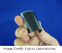
Fujitsu Laboratories Ltd. today announced the development of the world's first adhesive sheet composed of carbon nanotubes with extremely high thermal conductivity of up to 100 W/mK (watt per meter per Kelvin).
Carbon nanotubes have high thermal conductivity and represent a promising candidate for heat dissipation from heat sources including semiconductor devices. Nevertheless, the material remains difficult to handle due to its fragility, rendering it impractical for many purposes. To address this, Fujitsu has successfully developed a technology for laminating vertically aligned carbon nanotubes, while maintaining their original characteristics of high thermal conductivity and flexibility, as well as a technology for bonding them with sufficient adhesion. This technology facilitates the cutting and handling of carbon nanotube sheets, making it possible to use them as a heat dissipation material, for example, in automotive power modules for electric vehicles (EVs).
Fujitsu aims to license the use of its newly-developed carbon nanotube adhesive sheets to companies in the materials and electrical industries, and will continue to support their use in a variety of commercial applications.
Background and Development
EVs are increasingly being put to practical use as efforts to regulate greenhouse gases accelerate throughout the world. Despite this, the fact that EVs are more expensive than gasoline-powered vehicles and lack similar driving ranges continues to hinder their widespread adoption.
In order to improve cost-performance and driving range in recent years, efforts have been made to develop semiconductor devices that use silicon carbide or gallium nitride as an alternative material to the more commonly-used silicon to reduce the size, weight, power consumption, and cost of power modules for electric vehicles. In order to make this a reality, however, countermeasures to deal with heat generated around semiconductor devices due to module miniaturization must be resolved, and components such as heat dissipation materials and bonding materials that make up modules must be designed to achieve unprecedented levels of heat resistance and thermal conductivity.
Challenges
Carbon nanotubes, a type of nanotechnology material made from carbon atoms, have thermal conductivity that is about 10 times higher than copper. One potential use of this material is its use as a heat sink for dissipating heat from heat sources like semiconductor devices. In 2017, Fujitsu developed a high thermal conductivity sheet using carbon nanotubes, but in order to maintain the sheet shape, the sheet is sintered and molded at an ultra-high temperature of 2000 °C or higher, which results in a material that is inflexible. A hard sheet can be attached to flat materials, but it is not suitable for joining materials together that are uneven, which inhibits the places in which the sheet can be applied.
Furthermore, in areas around semiconductor devices where reliability is essential, it is necessary to bond both the semiconductor and heatsink via a heat dissipation sheet consisting of carbon nanotubes in order to follow the change in shape caused by temperature differences before and after the device is operated. In general, carbon nanotubes are made adhesive by mixing them into an adhesive material such as resin or rubber, forming a sheet. However, because these adhesive materials have low thermal conductivity, it has been extremely difficult to achieve sufficient levels of both thermal conductivity and adhesion.
About the Newly Developed Technology
Fujitsu has developed the world's first carbon nanotube adhesive sheet that exhibits extremely high thermal conductivity of up to 100 W/mK even when interface resistance is included.
The features of the developed technology are as follows.
- Sheet Laminate Technology Fujitsu has developed a technique for laminating vertically aligned carbon nanotubes while maintaining the alignment. The laminate layer consists of two layers, a protective sheet and an adhesive layer, and has a laminate structure in which the laminate layer protects the top and bottom of carbon nanotubes. Carbon nanotubes are difficult to use as heat dissipating materials because they easily lose their shape. However, this technology protects the carbon nanotubes themselves with a laminate layer, making them stable in shape and making cutting and handling easier, which was difficult with conventional technologies.
Figure1: Internal structure of carbon nanotube adhesive sheet
- High-Thermal-Conductivity Sheet Bonding Technology The adhesive layer that makes up the laminate layer is made of a polymer that is several microns thick. Because even a small amount of resin can cause large thermal resistance, it has become an issue that must be solved to achieve both adhesiveness and thermal conductivity. Thus, by optimizing three or more correlation parameters, such as the density of carbon nanotubes, the type and thickness of the resin, and the bonding conditions, utilizing knowledge of thermal resistance at the interface between carbon nanotubes and resins cultivated over many years, it becomes possible to bond carbon nanotubes while maintaining sufficient adhesive properties without impairing thermal conductivity.
Effects
The newly developed carbon nanotube adhesive sheet has thermal conductivity of up to 3 times that of the conventional indium heat dissipation material, which is known as a high thermal conductivity material, compared with measured values including interface resistance.
Since the sheet is laminated with adhesive and protective layers, it can be easily cut and handled, and can be used for applications requiring adhesion.
These technologies will make it possible to put carbon nanotubes into practical use as heat dissipating materials, including in automotive power modules for EVs.
Future Plans
Going forward, Fujitsu Laboratories will license the use of its carbon nanotube adhesive sheets to companies in the materials and electrical industries. and will continue to support their commercialization and practical use.


