


 American Made Advocacy: Rebuilding America’s Military Stockpiles Begins With Microelectronics
 The Right Approach: The End of an Era—DoD Proposes MIL-PRF-31032 Cancellation
 Defense Speak Interpreted: Hypersonics Report Back After Six Years of Silence


Pasternack Launches Seven New Fixed Load VNA Calibration Kits
June 1, 2020 | PasternackEstimated reading time: 1 minute
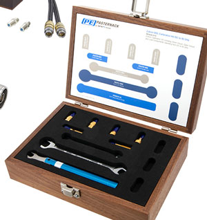
Pasternack, an Infinite Electronics brand and a leading provider of RF, microwave and millimeter wave products, has just released a new line of short-open-load-through (SOLT) calibration kits that are ideal for use in test and measurement, lab and RF & Microwave production test applications.
Pasternack’s expanded line of VNA calibration kits are available in 12 versions including short circuit, open circuit and load kits (SOL) as well as short circuit, open circuit, load and thru kits (SOLT) with 2.4mm, 2.92mm, 3.5mm, 7/16 DIN, 7mm, BNC and N-Type interface options.
Each of these new VNA calibration kits from Pasternack include all of the necessary short circuit, open circuit, loads and thru (model dependent) components required for VNA calibration. The kits are suitable for many vector network analyzers from the industry’s leading providers such as Agilent, Rohde & Schwarz, Anritsu and Copper Mountain. These RF test and measurement kits come packaged in protective wooden boxes.
The new SOLT calibration kits offer excellent performance characteristics that are specially designed for the fine-tuning and calibration of sensitive test equipment in engineering labs, production environments and quality testing facilities. Every Pasternack calibration kit is built to withstand years of rigorous use and provides accurate RF equipment calibration for the life of the product.
“A properly calibrated VNA is required for precise characterization of RF and microwave components used in a myriad of industries and applications. These new SOLT calibration kits provide the precision components that are essential to perform accurate analyzer calibrations,” said Steve Ellis, Interconnect Product Line Manager at Pasternack.
Share on:


Testimonial
"In a year when every marketing dollar mattered, I chose to keep I-Connect007 in our 2025 plan. Their commitment to high-quality, insightful content aligns with Koh Young’s values and helps readers navigate a changing industry. "
Brent Fischthal - Koh YoungSuggested Items
Driving Innovation: Selecting the Right Laser Source
04/28/2026 | Simon Khesin -- Column: Driving InnovationWhen I first joined Schmoll Maschinen, I brought experience from almost every PCB process, except for laser. As I immersed myself in laser processing, I realized why it can seem so daunting to a newcomer. The complexity arises from three intersecting factors: A vast variety of laser sources: CO2, UV-nano, green-pico, UV-pico, IR-pico, and others; a diverse range of applications: Drilling, cutting, ablation, and more; and an extensive list of materials: These have vastly different absorption rates. Choosing the right machine or laser source is rarely trivial. Even for experienced engineers, answering "Which source is best?" requires examining the business's specific goals.
Institute of Circuit Technology Spring Seminar 2026: A Bright Future in Europe
04/23/2026 | Pete Starkey, I-Connect007Through the leafy lanes and spring flowers of Warwickshire and back to Meridan, the traditional centre of England, and now officially part of the Metropolitan Borough of Solihull in the county of the West Midlands, I attended the Annual General Meeting and Spring Seminar of the Institute of Circuit Technology (ICT) on April 14. Out of the AGM came notable changes in leadership at the top of the Institute: the retirement of Mat Beadel as chair and Emma Hudson as technical director. Effective May 1, Steve Driver is the new chair, and Alun Morgan is the new technical director.
ACCM Unveils Negative and Near-zero CTE Materials for Large-Format AI Chips
04/21/2026 | Advanced Chip and Circuit MaterialsAdvanced Chip and Circuit Materials, Inc. (ACCM) has launched two new materials: Celeritas HM50, with a negative coefficient of thermal expansion (CTE) of -8 ppm/°C to offset the positive CTE and expansion of copper with temperature on circuit boards, and Celeritas HM001, with near-zero CTE and the low-loss performance needed for high-speed signal layers to 224 Gb/s and faster in artificial intelligence (AI) circuits.
Fresh PCB Concepts: Designing PCBs for Harsh Environments—Reliability Is Engineered Upstream
04/23/2026 | Team NCAB -- Column: Fresh PCB ConceptsWhen engineers hear the phrase “harsh environment,” they usually think of the extreme temperature swings, vibration and shock, pressure changes, or radiation in aerospace. However, aerospace is not the only harsh environment where electronic assemblies must survive. Automotive power electronics, downhole oil and gas tools, marine controls, rail systems, defense platforms, and industrial automation equipment all expose PCBs to environments that are equally unforgiving. The stress mechanisms may differ, but the physics does not.
Advanced Packaging for AI: Reliability Starts at the Cu/Cu/Cu Microvia Junction
04/20/2026 | Kuldip Johal, MKS' AtotechThe rapid growth of AI computing, from training clusters to inference at scale, is reshaping demand across the entire electronics supply chain. Advances in technology requirements, such as higher bandwidth, lower latency, and greater compute density, are driving the development of advanced packaging technologies and transforming the PCB industry across design, manufacturing, testing, and even architecture.