


 Global PCB Connections: Rigid-flex and Flexible PCBs—The Backbone of Modern Electronics
 Flexible Thinking: The Key to a Successful Flex Circuit Design Transfer
 Happy’s Tech Talk #29: Bend-to-Install Semi-flex FR-4


HARTING’s Component Carrier Can Replace Flexible PCBs
July 15, 2020 | PR NewswireEstimated reading time: 4 minutes
Flexible printed circuit boards made of thin polyimide films have established themselves in many product areas thanks to their application flexibility. Populating and assembling them, however, is decidedly more complex. This is where a newly developed component carrier from HARTING enters the picture.
A standardised component carrier for electronic components
By harnessing this all new HARTING development, electronic components can be fitted directly onto the component carrier, thereby replacing flexible circuit boards. The component carrier serves as a connecting element between the printed circuit board (PCB) and electronic components such as LEDs, ICs, photodiodes and sensors.
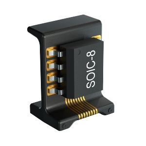
The populated component carriers are delivered in tape & reel. In their standard design, the carriers can be processed in automatic assembly systems, just like other SMD electronic components. Two different sizes are currently available and can accommodate electronic components of standard size SOIC-8 and smaller. Moreover, HARTING can also produce the carriers in customer-specific sizes.
HARTING has identified three example applications where the component carrier can replace flexible circuit boards:
- Components at a 90° angle to the circuit board: The component carrier is suitable for scenarios in which electrical components, such as sensors, need to be positioned normal to the circuit board. The automatic assembly process enables the placement of temperature sensors or hall sensors on the carrier to a high degree of accuracy, which in turn results in precise, reproducible measurements. Optical components are another salient example, such as LEDs or photodiodes used to generate precise light barriers.
- Clearance from the circuit board: The component carrier also makes it possible to maintain a clearance between the circuit board and an electronic component. Consequently, a temperature sensor can be used to measure the temperature in the housing without being influenced by the waste heat from other components on the PCB. It also means that an LED can be placed clear of the circuit board, thereby avoiding the risk of surrounding components casting shadows.
- Antenna function: The component carrier can be manufactured using different base polymers. In this way, different antenna material properties can be factored in, such as dielectric constant and loss factor. The specific antenna layout can be used for various applications in the MHz and GHz frequency range, such as Bluetooth, WiFi, ZigBee and 5G.
3D-MID technology as an alternative to flexible PCBs
Thanks to the 3D-MID (mechatronic integrated device) technology, electronic components can be fitted directly onto a three-dimensional body without the need for circuit boards or connecting cables. The base body is produced through injection moulding, whereby the thermoplastic is provided with a non-conductive, inorganic additive. In order for this material to be able to accommodate electrical circuits, the additives in the plastic are "activated" through laser direct structuring (LDS). In this process, the laser beam writes the areas intended for the conductive tracks and creates a micro-rough structure. The metal particles released in the process form the nuclei for the subsequent chemical metallisation.
This process creates electrical traces across the three-dimensional base body. The plastic employed offers high thermal stability and can therefore be soldered in the reflow oven.
HARTING has been implementing the entire 3D-MID process chain in-house for over 10 years, from the project idea to the populated series product. The technology is finding use in application scenarios in areas such as medical technology, industrial electronics and consumer electronics and all the way through to safety-related components in the automotive industry. The HARTING 3D-MID business unit is the largest provider of 3D-MID components outside of Asia.
The component carrier developed by this process is suitable for various applications. It can be equipped with several sensors that, if desired, could be aligned in three directions to take measurements in three axes (X, Y, Z). Components can be fitted simultaneously on two parallel surfaces on the front and back sides, as well as on the end face. HARTING has submitted a patent application for the component carrier.
The component carrier cuts costs by two-thirds
In an automated process, HARTING fits electronic components such as LEDs, ICs, photodiodes and sensors directly on the component carrier. The total cost of the component carrier is two-thirds lower than those of flexible PCB solutions. This is due to the fact that it eliminates the frequently complex handling involved with flexible printed circuit boards, e.g. populating, gluing and assembling. The process even delivers benefits in small volumes, as the component carrier can be used for different applications without adaptation, thereby eliminating the costs of a new injection mould. Compared with flexible printed circuit boards, this process achieves more precise component positioning, greater repeatability and better quality.
HARTING has identified another advantage of the component carrier, namely the short timeframe required to deliver finished components. Since the plastic carrier remains unchanged, all that is needed are specifications for placement of the electronic components. Experts in 3D-MID can use this to create a production-optimised layout proposal. Adjustments of the laser program are all that is needed to tailor the electrical traces to the respective application. Once the customer has approved the product and components have been received, initial production samples can be dispatched within two to three weeks – and even faster, if necessary.
Share on:


Testimonial
"The I-Connect007 team is outstanding—kind, responsive, and a true marketing partner. Their design team created fresh, eye-catching ads, and their editorial support polished our content to let our brand shine. Thank you all! "
Sweeney Ng - CEE PCBSuggested Items
Partnerships Drive Innovation for a Brighter Manufacturing Future
08/26/2025 | Barry Matties, I-Connect007When Schweitzer Engineering Laboratories (SEL) opened its greenfield facility in 2023, it did so with careful attention to choosing its suppliers. In this discussion, Collin Peters, electronics business director for North America at MKS’ Atotech, and Justin Kennedy, manager of engineering at SEL, explore their unique partnership that includes collaborative efforts to develop innovative solutions like the Uniplate® PLBCu6 line.
The Art and Science of PCB Floor Planning: A Comprehensive Guide
08/14/2025 | Cory Grunwald and Jeff Reinhold, Monsoon SolutionsPCB design is an intricate and crucial part of developing electronic products. One of the foundational stages of PCB design is floor planning, a phase where the placement of components and the flow of signals are meticulously mapped out. A good floor plan ensures that the PCB performs well, is easy to manufacture, and meets all mechanical and electrical requirements. We’ll explore the essential aspects of floor planning, from its objectives and process to the challenges that designers face.
Advint and SanRex Expand High-Performance DC Rectifier Access for North American PCB Fabricators
08/12/2025 | Advint IncorporatedAdvint Incorporated has entered a strategic partnership with SanRex Corporation, enhancing access to industrial-grade DC rectifiers for the US printed circuit board industry. With a legacy of power innovation and performance across the globe, SanRex rectifiers are available through Advint’s proficient distribution network.
Advint and Sayron Bring Advanced Rectifier Solutions to High-Reliability PCB Manufacturers
08/01/2025 | Advint IncorporatedAdvint Incorporated has partnered with Sayron, a leading global rectifier manufacturer, to supply cutting-edge IGBT-based DC rectifiers to high-performance PCB manufacturers across North America and beyond. Sayron’s precision-engineered rectifiers align with the stringent requirements of advanced PCB processes.
Trouble in Your Tank: Metallizing Flexible Circuit Materials—Mitigating Deposit Stress
08/04/2025 | Michael Carano -- Column: Trouble in Your TankMetallizing materials, such as polyimide used for flexible circuitry and high-reliability multilayer printed wiring boards, provide a significant challenge for process engineers. Conventional electroless copper systems often require pre-treatments with hazardous chemicals or have a small process window to achieve uniform coverage without blistering. It all boils down to enhancing the adhesion of the thin film of electroless copper to these smooth surfaces.