


 The Knowledge Base: A Conference for Cleaning and Coating of Mission-critical Electronics
 Defense Speak Interpreted: Is DARPA Still Around After CHIPS?
 Beyond the Board: Orbital High Ground—Why Space Superiority Is Slipping Away


STI Electronics to Attend 2020 Space & Missile Defense Symposium
July 27, 2020 | STI Electronics, Inc.Estimated reading time: 1 minute
STI Electronics, Inc., a full service organization established in 1982, announces that it is a sponsor and an attendee of the Space & Missile Defense (SMD) Symposium. Scheduled to take place Tuesday, August 4, 2020 at 8 a.m. CST, the SMD Symposium is the leading educational, professional development and networking event for the space and missile defense community. This year, the event will be held virtually. For more information, visit https://smdsymposium.org.
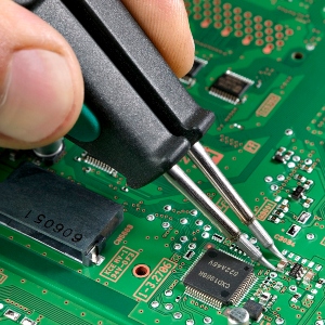
Engineering Services - STI Electronics’ manufacturing lab encompasses 26,000 sq. ft. of floor space containing a clean room, multiple surface mount lines, and multiple flexible work cells for final assembly, 7711/7721 certified rework and repair, box build, and test. The facility and equipment is complimented by a highly skilled and trained work force of electronic technicians and associates, all of whom are certified to the highest standard of IPC J-STD-001 ES (Space Addendum).
Box Build • Circuit Design • Designing for the Future • Design & Manufacturing • Electronics Assembly • Material Failure Analysis • Microelectronics Packaging • Rework & Repair • Testing
Training Services - Premier provider of training courses for the electronics assembly and related industries. STI offers a wide variety of electronic assembly and solder training courses ranging from commercial to high reliability requirements. STI is an IPC Authorized Training Center for Instructor and Operator level training for all IPC courses. STI can also customize training to fit a particular need.
Training Materials department provides solder training kits for J-STD-001, IPC-7711/7721 along with unique or custom training materials including Fine Pitch Lead Free Solder Training Kits. STI is also an approved distributor for IPC training materials and videos.
Assembly & Solder Kits • Customized Training Courses • Inspection Kits • IPC Approved Distributor • IPC Courses • SMT & PCB / IPC Training • NASA Courses
Share on:


Suggested Items
Driving Innovation: Direct Imaging vs. Conventional Exposure
07/01/2025 | Simon Khesin -- Column: Driving InnovationMy first camera used Kodak film. I even experimented with developing photos in the bathroom, though I usually dropped the film off at a Kodak center and received the prints two weeks later, only to discover that some images were out of focus or poorly framed. Today, every smartphone contains a high-quality camera capable of producing stunning images instantly.
Hands-On Demos Now Available for Apollo Seiko’s EF and AF Selective Soldering Lines
06/30/2025 | Apollo SeikoApollo Seiko, a leading innovator in soldering technology, is excited to spotlight its expanded lineup of EF and AF Series Selective Soldering Systems, now available for live demonstrations in its newly dedicated demo room.
Indium Corporation Expert to Present on Automotive and Industrial Solder Bonding Solutions at Global Electronics Association Workshop
06/26/2025 | IndiumIndium Corporation Principal Engineer, Advanced Materials, Andy Mackie, Ph.D., MSc, will deliver a technical presentation on innovative solder bonding solutions for automotive and industrial applications at the Global Electronics A
Fresh PCB Concepts: Assembly Challenges with Micro Components and Standard Solder Mask Practices
06/26/2025 | Team NCAB -- Column: Fresh PCB ConceptsMicro components have redefined what is possible in PCB design. With package sizes like 01005 and 0201 becoming more common in high-density layouts, designers are now expected to pack more performance into smaller spaces than ever before. While these advancements support miniaturization and functionality, they introduce new assembly challenges, particularly with traditional solder mask and legend application processes.
Knocking Down the Bone Pile: Tin Whisker Mitigation in Aerospace Applications, Part 3
06/25/2025 | Nash Bell -- Column: Knocking Down the Bone PileTin whiskers are slender, hair-like metallic growths that can develop on the surface of tin-plated electronic components. Typically measuring a few micrometers in diameter and growing several millimeters in length, they form through an electrochemical process influenced by environmental factors such as temperature variations, mechanical or compressive stress, and the aging of solder alloys.