


 It’s Only Common Sense: If You’re Not Differentiated, You’re Dead
 Alpha Insights, Performance by Design: The Future of PCB Manufacturing in the Midwest
 Happy’s Tech Talk #43: Engineering Statistics Training With Free Software


LPKF Delivers First AMP Laser System for Volume Manufacturing of IC Packages
October 8, 2020 | LPKFEstimated reading time: 2 minutes
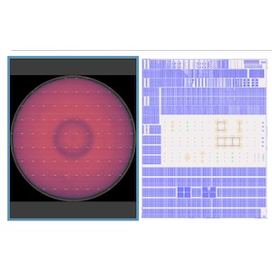
LPKF’s Active Mold Packaging (AMP) technology enables electrical circuits directly on the surface and inside the volume of the epoxy mold compound. This contributes to cost and space savings in advanced packaging manufacturing, and to a higher functional density of finished ICs. In addition, AMP helps to reduce power consumption, improves heat dissipation for power applications, enables additive 2L EMC-RDL formation and enables a whole suite of RF applications relevant for use in 5G. Taken together, these key factors contribute to a meaningful advance of the semiconductor industry. Starting now, the advantages made possible by AMP are leveraged by a large OEM manufacturer of integrated circuits in one of its production sites in South-East Asia. Together with LPKF, the company recently installed an LPKF system, which will make the AMP process available for high volume manufacturing in advanced packaging applications.
More than ever, innovative solutions for mounting and connection technology are crucial factors in the semiconductor industry. Functional integration of the kind made possible by AMP technology is another signifi-cant step towards this goal. Active Mold Packaging simplifies integrated circuits (ICs) and systems-in-package (SiPs), and it increases value add for the users. When using AMP, the epoxy molding compound (EMC) – previously used only to protect ICs or SiPs – is converted into an active carrier of electrical functionality. The simple, time-saving, and reliable 2.5D packaging approach of AMP is based on three proven and standardized electronic production technologies: EMC encapsulation, laser processing using laser direct structuring (LDS), and selective metallization of the laser-processed areas with copper.
A new class of epoxy molding compounds (EMCs) has been developed for the laser direct structuring (LDS) process and is available in granulate and tablet form from a selection of well-known suppliers. In addition, this material is well suited for the plating process. In this process, laser direct structuring can reach a resolution range of 25µm for each linewidth and space.
Active Mold Packaging enables direct, electrically conducting connections between active and passive components in an IC or SiP. This shortens electrical path lengths and thus ohmic resistance and induct-ance.
Target applications of AMP are currently being developed for the 5G technology segment, and also for “beyond 5G” (B5G) – or 6G – RF technologies. They can apply to a wide range of uses: mmWave antennae as antenna-in/on-package (AiP/AoP) modules that operate in ISM bands at e.g. 24 GHz, 61 GHz, and 121 GHz, vehicle radar modules that operate between 76 GHz and 81 GHz, 5G amplifiers, or even EMI shielding. Other applications are package-on-package (PoP), 2L interposers, multi-chip modules (MCMs), thermal management and SiP connections.
Share on:


Testimonial
"Advertising in PCB007 Magazine has been a great way to showcase our bare board testers to the right audience. The I-Connect007 team makes the process smooth and professional. We’re proud to be featured in such a trusted publication."
Klaus Koziol - atgSuggested Items
Nolan’s Notes: Tariffs, Technologies, and Optimization
10/01/2025 | Nolan Johnson -- Column: Nolan's NotesLast month, SMT007 Magazine spotlighted India, and boy, did we pick a good time to do so. Tariff and trade news involving India was breaking like a storm surge. The U.S. tariffs shifted India from one of the most favorable trade agreements to the least favorable. Electronics continue to be exempt for the time being, but lest you think that we’re free and clear because we manufacture electronics, steel and aluminum are specifically called out at the 50% tariff levels.
MacDermid Alpha & Graphic PLC Lead UK’s First Horizontal Electroless Copper Installation
09/30/2025 | MacDermid Alpha & Graphic PLCMacDermid Alpha Electronics Solutions, a leading supplier of integrated materials and chemistries to the electronics industry, is proud to support Graphic PLC, a Somacis company, with the installation of the first horizontal electroless copper metallization process in the UK.
Electrodeposited Copper Foils Market to Grow by $11.7 Billion Over 2025-2032
09/18/2025 | Globe NewswireThe global electrodeposited copper foils market is poised for dynamic growth, driven by the rising adoption in advanced electronics and renewable energy storage solutions.
MacDermid Alpha Showcases Advanced Interconnect Solutions at PCIM Asia 2025
09/18/2025 | MacDermid Alpha Electronics SolutionsMacDermid Alpha Electronic Solutions, a global leader in materials for power electronics and semiconductor assembly, will showcase its latest interconnect innovations in electronic interconnect materials at PCIM Asia 2025, held from September 24 to 26 at the Shanghai New International Expo Centre, Booth N5-E30
Trouble in Your Tank: Implementing Direct Metallization in Advanced Substrate Packaging
09/15/2025 | Michael Carano -- Column: Trouble in Your TankDirect metallization systems based on conductive graphite are gaining popularity throughout the world. The environmental and productivity gains achievable with this process are outstanding. Direct metallization reduces the costs of compliance, waste treatment, and legal issues related to chemical exposure. A graphite-based direct plate system has been devised to address these needs.