


 Global PCB Connections: Rigid-flex and Flexible PCBs—The Backbone of Modern Electronics
 Flexible Thinking: The Key to a Successful Flex Circuit Design Transfer
 Happy’s Tech Talk #29: Bend-to-Install Semi-flex FR-4


MKS Expands Industry Footprint in Asia with Newest HDI PCB Laser Manufacturing Solution
December 10, 2020 | MKS Instruments, Inc.Estimated reading time: 2 minutes
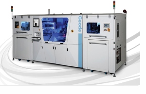
MKS Instruments, Inc., a global provider of technologies that enable advanced processes and improve productivity, announced it has received an order for multiple ESI® Geode™ HDI via drilling systems in Taiwan from a major technology leader in the HDI PCB manufacturing market.
“The market is embracing the economic advantages that the latest MKS developments have to offer,” said John Williams, Vice President and General Manager of MKS’ Equipment and Solutions division. “Our Geode HDI via drilling system meets the needs of high-volume HDI PCB manufacturing, while helping customers secure a technological advantage for current and future product requirements.”
This multi-unit order will support the customer’s existing manufacturing and future technological development through the use of leading-edge via drilling technology. Since its release to the market, the Geode HDI via drilling system has introduced HDI manufacturers to the performance advantages that ESI technology has provided to Flex PCB manufacturers for decades. The Geode platform has seen strong traction amongst the industry’s top players since its recent introduction to the market.
Developed by MKS’ Equipment & Solutions Division, already a market leader in flex PCB laser drilling solutions, the Geode system is optimized to process the rigid HDI PCBs and package substrates widely used in consumer electronics, such as smartphones and other handheld devices. Building on MKS’ technology leadership in laser processing for flexible printed circuits, Geode’s new laser technology and control capabilities deliver breakthrough performance. Its superior throughput, refined power control and small system footprint meet the needs of high-volume PCB manufacturers and technology leaders.
About MKS Instruments
MKS Instruments, Inc. is a global provider of instruments, systems, subsystems and process control solutions that measure, monitor, deliver, analyze, power and control critical parameters of advanced manufacturing processes to improve process performance and productivity for our customers. Our products are derived from our core competencies in pressure measurement and control, flow measurement and control, gas and vapor delivery, gas composition analysis, electronic control technology, reactive gas generation and delivery, power generation and delivery, vacuum technology, lasers, photonics, optics, precision motion control, vibration control and laser-based manufacturing systems solutions. We also provide services relating to the maintenance and repair of our products, installation services and training. Our primary served markets include semiconductor, industrial technologies, life and health sciences, research and defense. Additional information can be found at www.mksinst.com.
About the ESI Brand
ESI® is a brand within the MKS Instruments Equipment & Solutions Division. The ESI portfolio consists of laser-based micro manufacturing systems and component test systems that are used worldwide by manufacturers in the electronics industry to process the materials and components that are an integral part of the electronic devices and systems in use today. Leveraging over 40 years of laser-material interaction expertise and applied laser technology, ESI solutions enable customers to optimize production by providing more control, greater application flexibility and more precise processing of a wide range of materials. The result is higher production quality, increased throughput and higher back-end yields at a lower total cost-of-ownership. Additional information can be found at www.esi.com.
Share on:


Suggested Items
Kitron Wins Additional €7 Million Contract, Expanding Presence in Industrial Automation
06/06/2025 | KitronKitron has signed a significant manufacturing agreement with a leading customer in the industrial automation sector. The agreement covers electronics manufacturing services for a new generation of high-performance drive modules used in automation and motion control systems.
I-Connect007 Editor’s Choice: Five Must-Reads for the Week
06/06/2025 | Nolan Johnson, I-Connect007Maybe you’ve noticed that I’ve been taking to social media lately to about my five must-reads of the week. It’s just another way we’re sharing our curated content with you. I pay special attention to what’s happening in our industry, and I can help you know what’s most important to read about each week. Follow me (and I-Connect007) on LinkedIn to see these and other updates.
New Companion Guide to ‘DFM Essentials’ Delivers Deeper, Practical PCB Design Insights
06/05/2025 | I-Connect007The Companion Guide to DFM Essentials: Tips for Designing for Manufacturing is now available for free download. Building on the popular Printed Circuit Designer’s Guide to... DFM Essentials, this new resource from American Standard Circuits and ASC Sunstone Circuits offers advanced, real-world guidance to help PCB designers streamline production and avoid costly pitfalls.
Orbel Corporation Integrates Schmoll Direct Imaging
06/04/2025 | Schmoll AmericaOrbel Corporation in Easton, PA, proudly becomes the first PCM facility in the U.S. equipped with Schmoll’s MDI Direct Imaging system. This installation empowers Orbel to support customers with greater precision and quality.
GlobalFoundries Announces $16B U.S. Investment to Reshore Essential Chip Manufacturing and Accelerate AI Growth
06/04/2025 | GlobalFoundriesGlobalFoundries, working with the Trump Administration and with support from leading technology companies aiming to onshore critical components of their supply chain, announced plans to invest $16 billion to expand its semiconductor manufacturing and advanced packaging capabilities across its facilities in New York and Vermont.