


 It’s Only Common Sense: If You’re Not Differentiated, You’re Dead
 Alpha Insights, Performance by Design: The Future of PCB Manufacturing in the Midwest
 Happy’s Tech Talk #43: Engineering Statistics Training With Free Software


Tower Semiconductor Participates in DARPA LUMOS program
January 5, 2021 | Globe NewswireEstimated reading time: Less than a minute
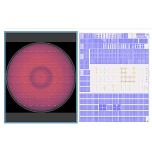
Tower Semiconductor, a leader in high-value analog semiconductor foundry solutions, announced that it is participating in the LUMOS program, with partial support from DARPA, to create a semiconductor foundry integrated-laser-on-silicon photonics process. This process will combine high-performance III-V laser diodes with Tower’s PH18 production silicon photonics platform. Multi-project wafer runs (MPW) will be coordinated with the new process, when ready. The initial versions of the PDK (process development kit) are expected in 2021 and will include laser and amplifier blocks.
The benefits of laser integration on silicon include an increase in the density of lasers, a reduction of coupling losses between the laser and the photonics, a reduction in components required, and a much-simplified packaging scheme. When combined with Tower’s rich suite of passive and active silicon photonics elements -- such as silicon and silicon-nitride waveguides, Mach-Zehnder modulators (MZM), and Ge photodiodes -- the co-integration will enable new products unavailable today from a volume semiconductor or photonics foundry.
The advanced process will be part of DARPA’s Lasers for Universal Microscale Optical Systems (LUMOS) program, which aims to bring high-performance lasers to advanced photonics platforms, addressing commercial and defense applications.
Share on:


Testimonial
"The I-Connect007 team is outstanding—kind, responsive, and a true marketing partner. Their design team created fresh, eye-catching ads, and their editorial support polished our content to let our brand shine. Thank you all! "
Sweeney Ng - CEE PCBSuggested Items
Taking Control of PCB Verification One Step at a Time
10/09/2025 | Kirk Fabbri, Siemens EDAToday’s designs are as complex as ever, and engineers face tough decisions every day. Simulation and verification teams are confronted with a three-fold challenge: understanding the underlying theory, mastering the tools, and applying best practices.Engineers need to navigate a vast and ever-changing cast of design and simulation tools, often with overlapping functionality.
Happy’s Tech Talk #43: Engineering Statistics Training With Free Software
10/06/2025 | Happy Holden -- Column: Happy’s Tech TalkIn over 50 years as a PCB process engineer, the one skill I acquired in college that has been most beneficial is engineering statistics. Basic statistics was part of my engineering fundamentals classes, but I petitioned the dean to let me take the engineering statistics graduate course because I was creating a senior thesis for my honors focus and needed more training on Design of Experiments (DOE).
Connect the Dots: Evolution of PCB Manufacturing—Lamination
10/02/2025 | Matt Stevenson -- Column: Connect the DotsWhen I wrote The Printed Circuit Designer's Guide to...™ Designing for Reality, it was not a one-and-done effort. Technology is advancing rapidly. Designing for the reality of PCB manufacturing will continue to evolve. That’s why I encourage designers to stay on top of the tools and processes used during production, to ensure their designs capitalize on the capabilities of their manufacturing partner.
Empower Sets New Benchmark with 20x Faster Response and Breakthrough Sustainability Demonstrated at OCP Global Summit 2025
09/25/2025 | Empower SemiconductorEmpower Semiconductor, the world leader in powering AI-class processors, announced that its Crescendo chipset, an artificial intelligence (AI) and high-performance computing (HPC) processor true vertical power delivery platform, is available now for final sampling, with mass production slated for late 2025.
Driving Innovation: Mastering Panel Warpage
09/23/2025 | Simon Khesin -- Column: Driving InnovationDuring the complex and multi-step process of PCB fabrication, a panel's flatness is constantly at risk. A host of factors can introduce warpage, bending, and unevenness, presenting a fundamental challenge to achieving high-precision results. This deformation (sometimes referred to as “bow and twist”), even on a microscopic scale, can lead to critical defects during subsequent stages, such as component surface mounting (e.g., tombstoning, solder opens) and the PCB's long-term functional reliability.