


 It’s Only Common Sense: If You’re Not Differentiated, You’re Dead
 Alpha Insights, Performance by Design: The Future of PCB Manufacturing in the Midwest
 Happy’s Tech Talk #43: Engineering Statistics Training With Free Software


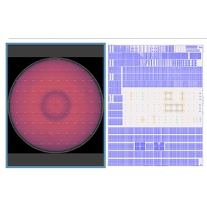
Surrey Unveils Breakthrough Manufacturing Process of Ultra-Thin Sensor for Smart Contact Lenses
January 12, 2021 | University of SurreyEstimated reading time: 1 minute
In a paper published by the journal Matter, engineers from the University of Surrey together with partners from Harvard University, University of Science and Technology of China, UK National Physical Laboratory, George Washington University and Zhejiang University Ningbo Research Institute report on how they have developed a breakthrough sensor system and manufacturing process.
The global team of engineers reveal that the new contact lens sensor system contains a photodetector for receiving optical information, a temperature sensor for diagnosing potential corneal disease and a glucose sensor for directly monitoring the glucose levels in tear fluid.
Dr Shiqi Guo, the first author of this study and current postdoctoral research fellow at Harvard University, said, "Our ultra-thin sensor layer is different from the conventional smart contact lenses -- with their rigid or bulk sensors and circuit chips that are sandwiched between two contact lens layers and make contact with tear fluids via microfluidic sensing channels. This new layer could instead be mounted onto a contact lens and maintain direct contact with tears, thanks to its easy assembly, high detection sensitivity, good biocompatibility and mechanical robustness; further, it doesn’t interfere with either blinking or vision."
Professor Sheng Zhang, co-author from Zhejiang University, said, "This multifunctional contact lens with field-effect transistors can provide diversified signals from eyes, which could be combined with advanced data analysis algorithms to provide personalised and accurate medical analysis for users. This kind of research will also become one of the major research directions at the Ningbo Research Institute."
Dr Yunlong Zhao, the corresponding author of this study and Lecturer in Energy Storage and Bioelectronics at the Advanced Technology Institute(ATI), University of Surrey, said: "The COVID-19 pandemic has had an enormous impact on the entire scientific community, with many of us asking how our work could help those suffering from similar future medical emergencies. We are confident that devices that utilise our sensor layer system could be used as a non-invasive way to help monitor and diagnose people’s health. Our results provide not only a unique and simple method for manufacturing advanced smart contact lenses but also novel insight for designing other multifunctional electronics for human-machine interface."
Read the full study here.
Share on:


Testimonial
"The I-Connect007 team is outstanding—kind, responsive, and a true marketing partner. Their design team created fresh, eye-catching ads, and their editorial support polished our content to let our brand shine. Thank you all! "
Sweeney Ng - CEE PCBSuggested Items
Beyond Thermal Conductivity: Exploring Polymer-based TIM Strategies for High-power-density Electronics
10/13/2025 | Padmanabha Shakthivelu and Nico Bruijnis, MacDermid Alpha Electronics SolutionsAs power density and thermal loads continue to increase, effective thermal management becomes increasingly important. Rapid and efficient heat transfer from power semiconductor chip packages is essential for achieving optimal performance and ensuring long-term reliability of temperature-sensitive components. This is particularly crucial in power systems that support advanced applications such as green energy generation, electric vehicles, aerospace, and defense, along with high-speed computing for data centers and artificial intelligence (AI).
Bluepath Robotics Optimizes AMR Fleets with Inductive Charging Solution from Wiferion
10/09/2025 | WiferionIn a dynamic and highly competitive industry such as logistics, efficient and uninterrupted material flows are of crucial importance. To ensure maximum uptime for its robots, Bluepath Robotics, which specializes in autonomous mobile robots (AMR), needed a reliable and powerful power supply.
‘Create your Connections’ – Rehm at productronica 2025 in Munich
10/08/2025 | Rehm Thermal SystemsThe electronics industry is undergoing dynamic transformation: smart production lines, sustainability, artificial intelligence, and sensor technologies dominate current discussions.
ESD Alliance Reports Electronic System Design Industry Posts $5.1 Billion in Revenue in Q2 2025
10/06/2025 | SEMIElectronic System Design (ESD) industry revenue increased 8.6% to $5,089.4 million in the second quarter of 2025 from the $4,685.5 million registered in the second quarter of 2024, the ESD Alliance, a SEMI Technology Community, announced in its latest Electronic Design Market Data (EDMD) report.
Rehm Optimizes Customer Service with a Digital Ticket System
10/02/2025 | Rehm Thermal SystemsKnowledge management and transparency are becoming increasingly important for productivity and quality in customer service.