-
- News
- Books
Featured Books
- I-Connect007 Magazine
Latest Issues
Current Issue
Signal Integrity & Metallization
Signal integrity and additive manufacturing, particularly metallization, are hot topics in PCB design and fabrication. PCB layouts are carefully engineered to achieve specific electrical and power performance targets.
Beyond the Rulebook
What happens when the rule book is no longer useful, or worse, was never written in the first place? In today’s fast-moving electronics landscape, we’re increasingly asked to design and build what has no precedent, no proven path, and no tidy checklist to follow. This is where “Design for Invention” begins.
March Madness
From the growing role of AI in design tools to the challenge of managing cumulative tolerances, these articles in this issue examine the technical details, design choices, and manufacturing considerations that determine whether a board works as intended.
- Articles
- Columns
- Links
- Media kit
||| MENU - I-Connect007 Magazine
LPKF ProtoLaser H4 Accelerates PCB Prototyping
September 12, 2022 | LPKFEstimated reading time: 2 minutes
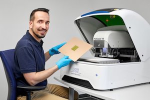
The ProtoLaser H4 has more than 45 years of experience in the mechanical processing of printed circuit boards and more than 30 years in laser processing. This experience is combined in the hardware and the LPKF CircuitPro system software included in the package. “The goal was a compact table-top system that would also convince the most demanding developers of electronics on different substrates. And it works,” says Lars Führmann, Sales Director LPKF DevelopmentQuipment with satisfaction. The new ProtoLaser is built on a granite base, has a powerful laser and a mechanical processing head that is operated independently from a tool magazine. During operation, laser safety class 1 applies - no special precautions are required.
With new tools, the production processes also change. With the ProtoLaser H4, the laser takes over the entire structuring of the fully coated circuit board materials. In this way, track/gap of 100 µm/50 µm can be reliably achieved. The drilling and cutting out of the circuit board or large breakthroughs is reserved for the mechanical tools. The ProtoLaser H4 integrates the tried-and-tested circuit board plotter into an innovative, high-precision system for laser micro-material processing.
A camera recognizes the exact position of the circuit board on the work table. This is how precise structuring of two-layer PCBs and single layers of multi-layers PCBs is possible. Flexible materials or foils are held securely in position with the integrated vacuum table.
The hardware achieves full performance with the easy-to-use system software. LPKF CircuitPro RP controls the entire production process - even for users without special expertise. Extensive libraries with material parameters, process flows for many common applications, a simple user interface and predefined laser tools simplify project planning. After loading the layout file, the software guides the user step by step through the production process. In-house prototyping significantly reduces the times of the individual design loops and is also suitable for small series.
Testimonial
"Advertising in PCB007 Magazine has been a great way to showcase our bare board testers to the right audience. The I-Connect007 team makes the process smooth and professional. We’re proud to be featured in such a trusted publication."
Klaus Koziol - atgSuggested Items
Kymeta Joins Red Cat Initiative for Maritime Connectivity
05/15/2026 | Globe NewswireRed Cat Holdings, Inc. , a U.S.-based provider of advanced all-domain drone and robotic solutions for defense and national security, announced that Kymeta, a world-leading flat-panel satellite terminal manufacturer, has joined the Red Cat Futures Initiative, the company’s industry-wide consortium accelerating advanced autonomous systems for modern warfare.
SPARK Microsystems Selected for CAD $1M in Government of Canada-backed FABrIC Funding
05/14/2026 | BUSINESS WIRESPARK Microsystems, a Canadian fabless semiconductor company specializing in next-generation short-range wireless communications, has been selected by FABrIC as a CAD $1 million grant recipient funded by the Government of Canada.
System Architecture Beyond the Die With Advanced Packaging as the Scaling Factor
05/14/2026 | Chetan Arvind Patil, Marvell TechnologyIn conventional monolithic semiconductor design, system integration was achieved within a single die and constrained by reticle limits. Compute cores, cache, memory controllers, and input output (I/O) interfaces were all co-optimized on a single process node, with performance closely tied to transistor density and on-die interconnect efficiency. This monolithic system-on-chip (SoC) approach enabled low-latency communication and relatively straightforward power delivery. However, as design for compute-intensive SoCs approaches reticle limits and advanced-node costs increase, the ability to continue scaling within a single die begins to diminish.
Rethinking Reinforcement Materials for Advanced Packaging
05/14/2026 | Ivana Ivanovic, Flexiramics B.V.Materials that once quietly supported the industry are now becoming limiting factors. The electronics industry is experiencing unprecedented pressure as RF systems push into mmWave frequencies, high-speed digital architectures advance into their next performance generation, and power densities climb across automotive, telecom, aerospace, and computing. Reinforcement materials, long treated as a background detail in laminate design, are suddenly at the centre of performance, reliability, and supply‑chain discussions.
Below the Surface: Active Component and Module Submounts—The Architecture Behind Performance
05/14/2026 | Chandra Gupta -- Column: Below the SurfaceIf you were to peel back the layers of a modern electronic system, such as a satellite transceiver, a LiDAR module, or a 5G base station, you would not immediately notice a specific component doing some of the most important work. It doesn’t amplify signals, emit light, or process data, yet without it, none of those functions would be stable, reliable, or scalable. That component is the active device submount.