


 American Made Advocacy: PCBs in the National Spotlight
 Defense Speak Interpreted: Extreme Financial Disparity in Drones and Missiles
 The Right Approach: The End of an Era—DoD Proposes MIL-PRF-31032 Cancellation


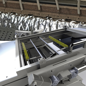
SEHO North America, Inc., a worldwide leading supplier of complete solutions for soldering processes and automated production lines, is one of the most innovative companies in the industry. Some of these innovations are aimed at taking cost-efficiency and energy-efficiency in the wave soldering process to a new level.
New pulsar emitters allow remarkably higher flexibility in the preheat area. Configuring emitters individually instead of using entire segments helps to realize the shortest distances between assemblies. Thus, there is virtually no wait time required between assemblies with different heat energy demands, ensuring highest energy-efficiency. This preheating concept allows for the cost-efficient and sustainable manufacture of large series as well as a batch size of one.
SEHO’s new automatic nozzle height adjustment provides higher flexibility in the soldering area of wave solder systems, particularly if a large number of different variants are to be manufactured. The height of each solder nozzle can be adjusted via the software, which allows creating the optimal product-specific distance between the circuit board and solder nozzle. This innovative function provides independence from the workpiece carrier or assembly design, a remarkably larger process window, maximum flexibility and process reliability.
Consistent height of the solder wave is crucial for wave soldering processes. SEHO provides the first automatic wave height measurement, built into the soldering section of the MWS 2300. This feature is based on a contact measurement that produces reliable results and processes for laminar as well as turbulent solder waves. Based on the measuring results, the wave height is automatically regulated within adjustable tolerances. The system thereby ensures the same height across the entire wave width at any time. The complete logging of all measured values and parameters also provides a proof of quality of the manufactured products.


