-
-
News
News Highlights
- Books
Featured Books
- pcb007 Magazine
Latest Issues
Current IssueSales: From Pitch to PO
From the first cold call to finally receiving that first purchase order, the July PCB007 Magazine breaks down some critical parts of the sales stack. To up your sales game, read on!
The Hole Truth: Via Integrity in an HDI World
From the drilled hole to registration across multiple sequential lamination cycles, to the quality of your copper plating, via reliability in an HDI world is becoming an ever-greater challenge. This month we look at “The Hole Truth,” from creating the “perfect” via to how you can assure via quality and reliability, the first time, every time.
In Pursuit of Perfection: Defect Reduction
For bare PCB board fabrication, defect reduction is a critical aspect of a company's bottom line profitability. In this issue, we examine how imaging, etching, and plating processes can provide information and insight into reducing defects and increasing yields.
- Articles
- Columns
- Links
- Media kit
||| MENU - pcb007 Magazine
Henniker Plasma: Plasma Treatment of Fluoropolymers
February 14, 2023 | Henniker PlasmaEstimated reading time: 2 minutes

PTFE, and other fluorinated polymers, are chemically inert, thermally stable and highly hydrophobic, due to their intrinsically low surface energy. The chemical inertness of PTFE as an example, means that it is virtually impossible to form lasting adhesive bonds and coatings tend instead to form droplets and 3D particles on the surface rather than a uniform film. Traditional methods to increase the surface energy involve the use of aggressive primers which represent an ecological hazard.
Fluorinated polymers are not readily modified by standard plasma processes. Oxygen plasmas, which are successfully used to treat many hydrocarbon-based polymers, are not successful because the binding energy of the fluorine to carbon atom is far higher than that of oxygen to carbon. Plasma treatment of fluorinated polymers with oxygen plasmas instead causes a gradual etching of the surface, as opposed to surface activation.
The use of hydrogen plasma on the other hand, produces an immediate and lasting change in the nature of the fluoropolymer surface. The action of atomic hydrogen, generated by the plasma, is to react with surface fluorine and remove this into the gas phase where it is pumped away by the vacuum system. Hydrogen then terminates the free surface bonds to produce a CHx polymer surface which is readily wettable. The resulting surface is also mildly-etched on a microscopic scale which produces a microscopically structured surface. Both actions in combination result in a modified surface which may be glued, painted etc.
Typical Results
Results, below and across, show the change in morphology, water contact angle and surface energy obtained for PTFE following hydrogen plasma treatment. The surface energy of PTFE that has been plasma treated is actually lower than that of many common polyolefins, such as polyethylene and polypropylene, and well within the range of wettability required for many adhesives to form strong bonds.
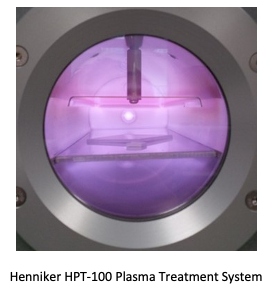
Plasma Process
When gas atoms are ionised, the collision of high energy particles knocks electrons out of their orbits. This results in the characteristic “glow” or light associated with plasma. Plasmas many different species including atoms, molecules, ions, electrons, free radicals, metastables, and photons in the short wave ultraviolet (vacuum UV or VUV) range. Plasmas are generated in closed vessels at low pressures, typically < 1.0 Torr. The low pressure results in a long mean free path of the plasma species, so that they remain reactive until contact with a surface. The overall chamber temperature at the commonly used power levels and pressures is close to room temperature
Testimonial
"In a year when every marketing dollar mattered, I chose to keep I-Connect007 in our 2025 plan. Their commitment to high-quality, insightful content aligns with Koh Young’s values and helps readers navigate a changing industry. "
Brent Fischthal - Koh YoungSuggested Items
Designers Notebook: Basic PCB Planning Criteria—Establishing Design Constraints
07/22/2025 | Vern Solberg -- Column: Designer's NotebookPrinted circuit board development flows more smoothly when all critical issues are predefined and understood from the start. As a basic planning strategy, the designer must first consider the product performance criteria, then determine the specific industry standards or specifications that the product must meet. Planning also includes a review of all significant issues that may affect the product’s manufacture, performance, reliability, overall quality, and safety.
Knocking Down the Bone Pile: Addressing End-of-life Component Solderability Issues, Part 4
07/16/2025 | Nash Bell -- Column: Knocking Down the Bone PileIn 1983, the Department of Defense identified that over 40% of military electronic system failures in the field were electrical, with approximately 50% attributed to poor solder connections. Investigations revealed that plated finishes, typically nickel or tin, were porous and non-intermetallic.
STMicroelectronics, Metalenz Sign a New License Agreement to Accelerate Metasurface Optics Adoption
07/14/2025 | STMicroelectronicsSTMicroelectronics, a global semiconductor leader serving customers across the spectrum of electronics applications and Metalenz, the pioneer of metasurface optics, announced a new license agreement.
Digital Twin Concept in Copper Electroplating Process Performance
07/11/2025 | Aga Franczak, Robrecht Belis, Elsyca N.V.PCB manufacturing involves transforming a design into a physical board while meeting specific requirements. Understanding these design specifications is crucial, as they directly impact the PCB's fabrication process, performance, and yield rate. One key design specification is copper thieving—the addition of “dummy” pads across the surface that are plated along with the features designed on the outer layers. The purpose of the process is to provide a uniform distribution of copper across the outer layers to make the plating current density and plating in the holes more uniform.
Global PCB Connections: Embedded Components—The Future of High-performance PCB Design
06/19/2025 | Jerome Larez -- Column: Global PCB ConnectionsA promising advancement in this space is the integration of embedded components directly within the PCB substrate. Embedded components—such as resistors, capacitors, and even semiconductors—can be placed within the internal layers of the PCB rather than mounted on the surface. This enables designers to maximize available real estate and improve performance, reliability, and manufacturability.