Ansys Joins TSMC's OIP Cloud Alliance for Secure Multiphysics Analysis in the Cloud
April 27, 2023 | ANSYSEstimated reading time: 1 minute

Ansys announced that it has joined TSMC's OIP Cloud Alliance to facilitate the deployment of fully distributed workflows for mutual customers. By driving toward the cloud interoperability of Ansys multiphysics solutions with TSMC's technology enablement, customers will easily be able to gain the full benefits of faster run times and elastic computing with major cloud vendors.
Combining EDA parallelism and cloud scalability, TSMC and its OIP Cloud Alliance partners are creating next-generation, cloud-optimized design methodologies to further accelerate turnaround time of critical design tasks. Ansys and other EDA partners will optimize their tools for multi-threaded, fully-distributed runs to best utilize cloud, while cloud partners will bring new virtual machines most suitable for the EDA workload of IC designs.
"Our customers of all sizes are leveraging the cloud to boost productivity while designing in TSMC's leading-edge technologies for new applications from high performance computing to mobile, artificial intelligence, networking, and 3D-IC," said Dan Kochpatcharin, head of the Design Infrastructure Management Division at TSMC. "By welcoming Ansys as the latest member into our OIP Cloud Alliance, TSMC aims to make Ansys' leading multiphysics signoff solutions available to all of our customers and help them bring their differentiated products to market sooner, with higher quality."
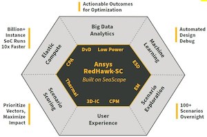
Ansys was an early adopter of elastic cloud computing with its SeaScape big-data platform – a cloud-native data infrastructure that was designed specifically for EDA. Ansys® RedHawk-SC™ was the first tool built to work with SeaScape (SC) and many other Ansys semiconductor tools have followed, including Ansys® PathFinder-SC™, Ansys® Totem-SC™, and Ansys® PowerArtist-SC™.
"Ansys' strategy for the future foresees an absolutely central role for cloud computing," said John Lee, vice president and general manager of the semiconductor, electronics, and optics business unit at Ansys. "We have invested heavily in cloud-enabled platforms that give our products clear advantages in speed and capacity over traditional tool environments that were not designed for the cloud."
Testimonial
"Our marketing partnership with I-Connect007 is already delivering. Just a day after our press release went live, we received a direct inquiry about our updated products!"
Rachael Temple - AlltematedSuggested Items
Setting Design Constraints Effectively
07/31/2025 | Stephen V. Chavez, Siemens EDAPCB design requires controlling energy within the medium of a PCB. The manner in which we control the chaos of energy is by implementing and utilizing physical and electrical rules, known as constraints, along with a specific structure and material(s) that make up what is known as the foundation of the design. These rules govern everything within the PCB structure and generally fall into two camps: performance and manufacturability. Setting this foundation correctly is extremely important and the key to success.
MacDermid Alpha Electronics Solutions Unveils Unified Global Website to Deepen Customer, Talent, and Stakeholder Engagement
07/31/2025 | MacDermid Alpha Electronics SolutionsMacDermid Alpha Electronics Solutions, the electronics business of Elements Solutions Inc, today launched macdermidalpha.com - a unified global website built to deepen digital engagement. The launch marks a significant milestone in the business’ ongoing commitment to delivering more meaningful, interactive, and impactful experiences for its customers, talent, and stakeholders worldwide.
Ansys 2025 R2 Enables Next-Level Productivity by Leveraging AI, Smart Automation, and Broader On-Demand Capabilities
07/30/2025 | PRNewswireAnsys, now part of Synopsys, announced 2025 R2, featuring new AI-powered capabilities across the portfolio that accelerate simulation and expand accessibility.
Connect the Dots: Sequential Lamination in HDI PCB Manufacturing
07/31/2025 | Matt Stevenson -- Column: Connect the DotsAs HDI technology becomes mainstream in high-speed and miniaturized electronics, understanding the PCB manufacturing process can help PCB design engineers create successful, cost-effective designs using advanced technologies. Designs that incorporate blind and buried vias, boards with space constraints, sensitive signal integrity requirements, or internal heat dissipation concerns are often candidates for HDI technology and usually require sequential lamination to satisfy the requirements.
Target Condition: The 5 Ws of PCB Design Constraints
07/29/2025 | Kelly Dack -- Column: Target ConditionHave you ever sat down to define PCB design constraints and found yourself staring at a settings window with more checkboxes than a tax form? You’re not alone. For many designers—especially those newer to the layout world—the task of setting up design constraints can feel like trying to write a novel in a language you just started learning.