


 Punching Out: 2024 North American PCB and EMS M&A Review
 Happy’s Tech Talk #37: New Ultra HDI Materials
 It’s Only Common Sense: When Data Isn’t Enough, Trust Your Gut


MKS Introduces ESI Geode A CO2 Laser System for High Precision and High-Speed ABF IC Substrate Manufacturing
May 31, 2023 | MKS Instruments, Inc.Estimated reading time: 1 minute
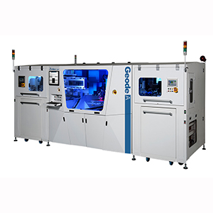
MKS Instruments, Inc., a global provider of technologies that transform our world, announced the official launch of the ESI Geode® A laser drill system today, a new configuration of the Geode® platform designed explicitly for drilling vias in the non-copper-clad ABF substrate market.
The Geode® A laser drilling system provides processing and application solutions for the FCBGA package substrate market, components which provide critical building blocks for everyday electronic devices and, in particular, high-performance computing. FCBGA substrates help enable supercomputing, artificial intelligence processing, autonomous cars, and other highly complex semiconductor modules.
“Manufacturers are under increased market pressure to deliver components that meet the precise demands of miniaturization and complexity required for advanced substrate manufacturing. At MKS, we are keenly focused on delivering the advanced technology needed for our customers to deliver next-generation productivity and quality,” said John Williams, MKS Vice President and General Manager of the ESI business. “In addition, the Geode® A laser drill is engineered as an integral component to the MKS Optimize the Interconnect SM solution, combining ESI laser drilling technologies with Atotech chemistry and plating equipment to provide customers with a full package of via formation technologies required to deliver optimal quality with the highest productivity for PCB and package substrate products.”
The Geode® A laser drilling system combines an innovative laser and optics configuration with precision pulse-shaping and beam-steering designed for ABF materials. These engineering innovations deliver the lowest cost of ownership and a greener manufacturing solution through 21% less floor space utilization, 72% less weight, and up to 65% less power consumption than the competition.
The Geode® A laser drilling system is available for purchase. More details can be found at www.esi.com, and system experts will be available at the JPCA 2023, Tokyo, Japan, May 31-June 2 in booth 6B-11.
Share on:


Suggested Items
Designers Notebook: Addressing Future Challenges for Designers
02/06/2025 | Vern Solberg -- Column: Designer's NotebookThe printed circuit board is and will probably continue to be the base platform for most electronics. With the proliferation of new generations of high I/O, fine-pitch surface mount semiconductor package variations, circuit interconnect is an insignificant factor. Circuit board designers continually face challenges such as component quantity and complexity, limited surface area, and meeting the circuit board’s cost target. The printed circuit design engineer’s prominent position demands the development of efficiently manufacturable products that perform without compromise.
DesignCon 2025, Day 2: It’s All About AI
01/30/2025 | Marcy LaRont, I-Connect007It’s hard to get away from the topic of artificial intelligence, but why would you? It’s everywhere and in everything, and my time attending presentations about AI at DesignCon 2025 was well worth it. The conference’s agenda featured engaging presentations and discussions focused on the technological advancements in AI, big data centers, and memory innovations, emphasizing the critical relationship between processors and circuit boards.
Beyond Design: Electro-optical Circuit Boards
01/22/2025 | Barry Olney -- Column: Beyond DesignPredicting the role of PCB designers in 10 years is a challenge. If only I had a crystal ball. However, we know that as technology progresses, the limitations of copper PCBs are increasingly apparent, particularly regarding speed, bandwidth, and signal integrity. Innovations such as optical interconnects and photonic integrated circuits are setting the stage for the next generation of PCBs, delivering higher performance and efficiency. The future of PCB design will probably incorporate these new technologies to address the challenges of traditional copper-based designs.
Designers Notebook: Impact of Advanced Semiconductor Packaging on PCB Stackup
01/07/2025 | Vern Solberg -- Column: Designer's NotebookTo accommodate new generations of high I/O semiconductor packaging, printed circuit board fabrication technology has had to undergo significant changes in both the process methods and the criteria for base material selection and construction sequence (stackup). Many of the new high-function multi-core semiconductor package families require more terminals than their predecessors, requiring a significantly narrower terminal pitch. Interconnecting these very fine-pitch, high I/O semiconductors to the PCB is made possible by an intermediate element referred to as an interposer.
BOOK EXCERPT: The Printed Circuit Designer’s Guide to... High Performance Materials, Chapter 4
01/02/2025 | I-Connect007In Chapter 4, Michael Gay discusses the two main types of copper foil used for PCB boards today: electrodeposited (ED) foil and rolled annealed (RA) foil. He also explains the pros and cons of each, and provides an update of the latest innovations in copper foil technology.